Methods and apparatus for off-axis lithographic illumination

a technology of lithographic illumination and off-axis direction, applied in the field of lithography, can solve the problems of imaging problems, future generations of deep ultraviolet lithography are expected to be and the process of deep ultraviolet lithography is currently limited to forming circuits

Inactive Publication Date: 2004-03-09
INTEL CORP
View PDF6 Cites 12 Cited by
  • Summary
  • Abstract
  • Description
  • Claims
  • Application Information

AI Technical Summary

Problems solved by technology

Generally, the deep ultraviolet lithography process is currently limited to forming circuits with geometries (also known as lines) of .about.100 nanometers.
Future generations of deep ultraviolet lithography are expected to be limited to forming circuits with some geometries of 50 nanometers.
This can cause the first order of the diffracted image to fall outside the projection lens, thereby causing imaging problems because both the zero and first diffraction orders must fall on the projection lens in order to properly resolve the image from the design plate.
Multiple illumination sources increases the size, cost and complexity of the lithography system.
Refraction becomes impractical as the wavelength becomes smaller, given the transmission properties of optical lenses degrade, and in fact absorb much of the light.
Blocking designs have been found to be inefficient.

Method used


Image

  • Methods and apparatus for off-axis lithographic illumination
  • Methods and apparatus for off-axis lithographic illumination
  • Methods and apparatus for off-axis lithographic illumination

Examples


Embodiment Construction

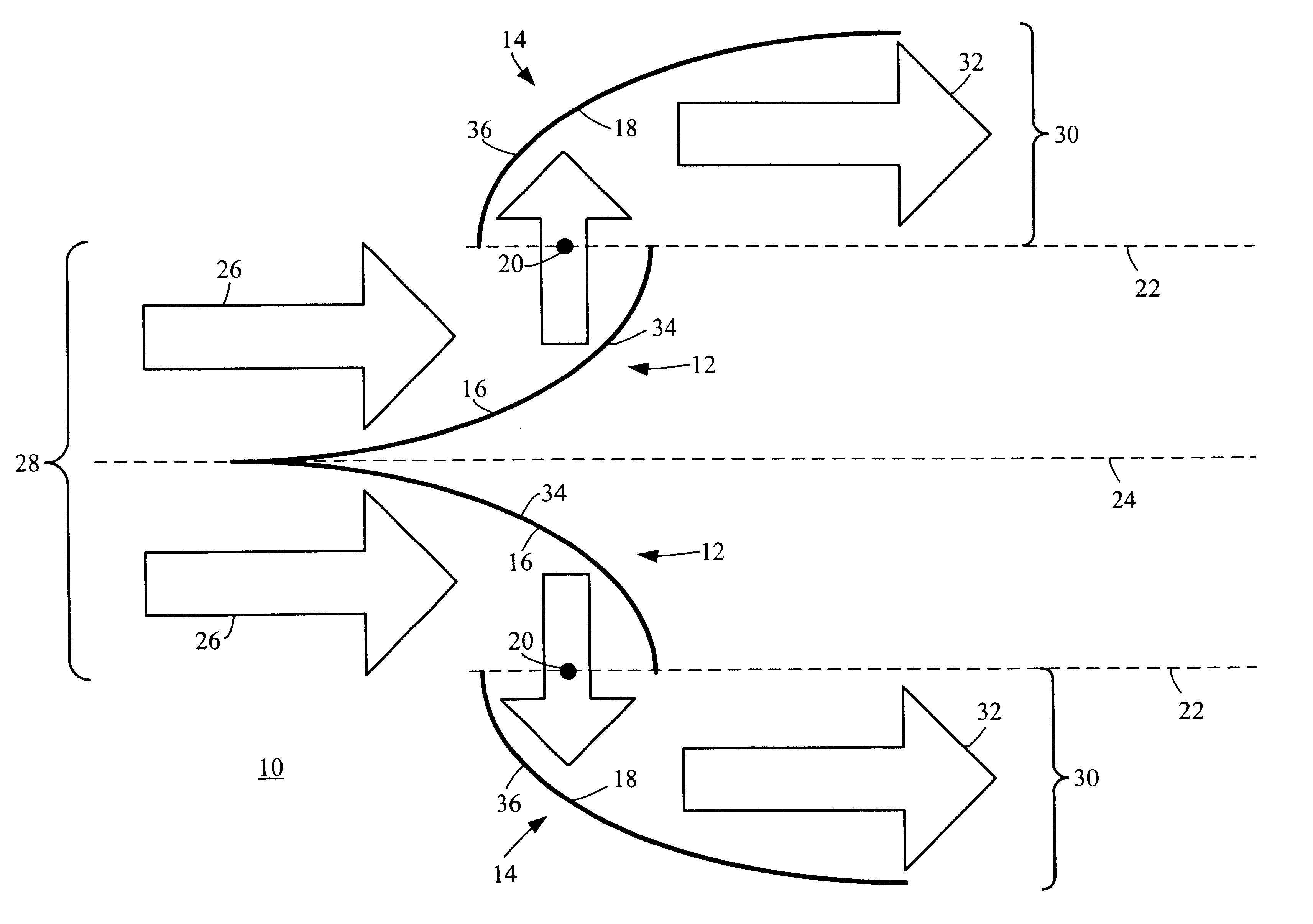
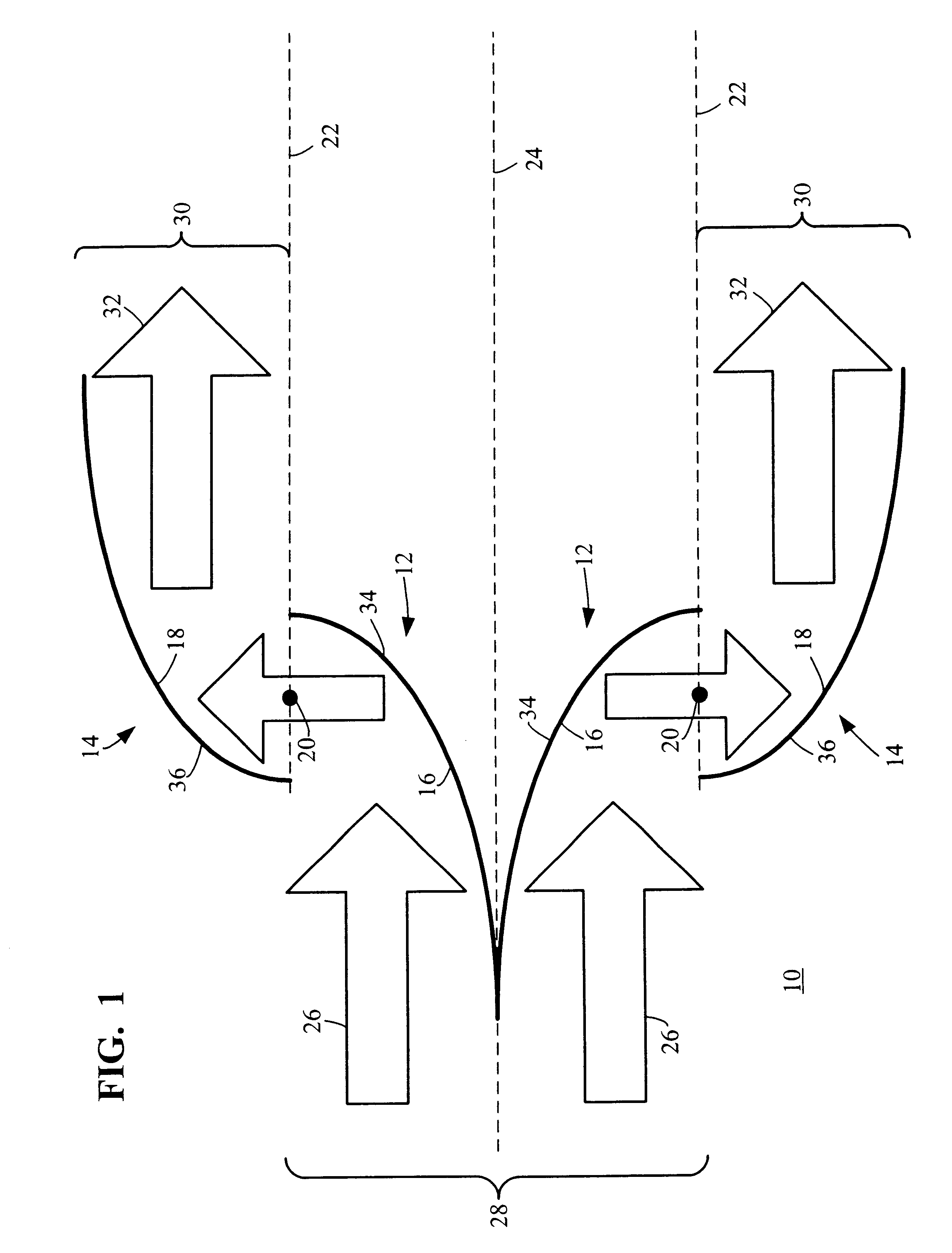
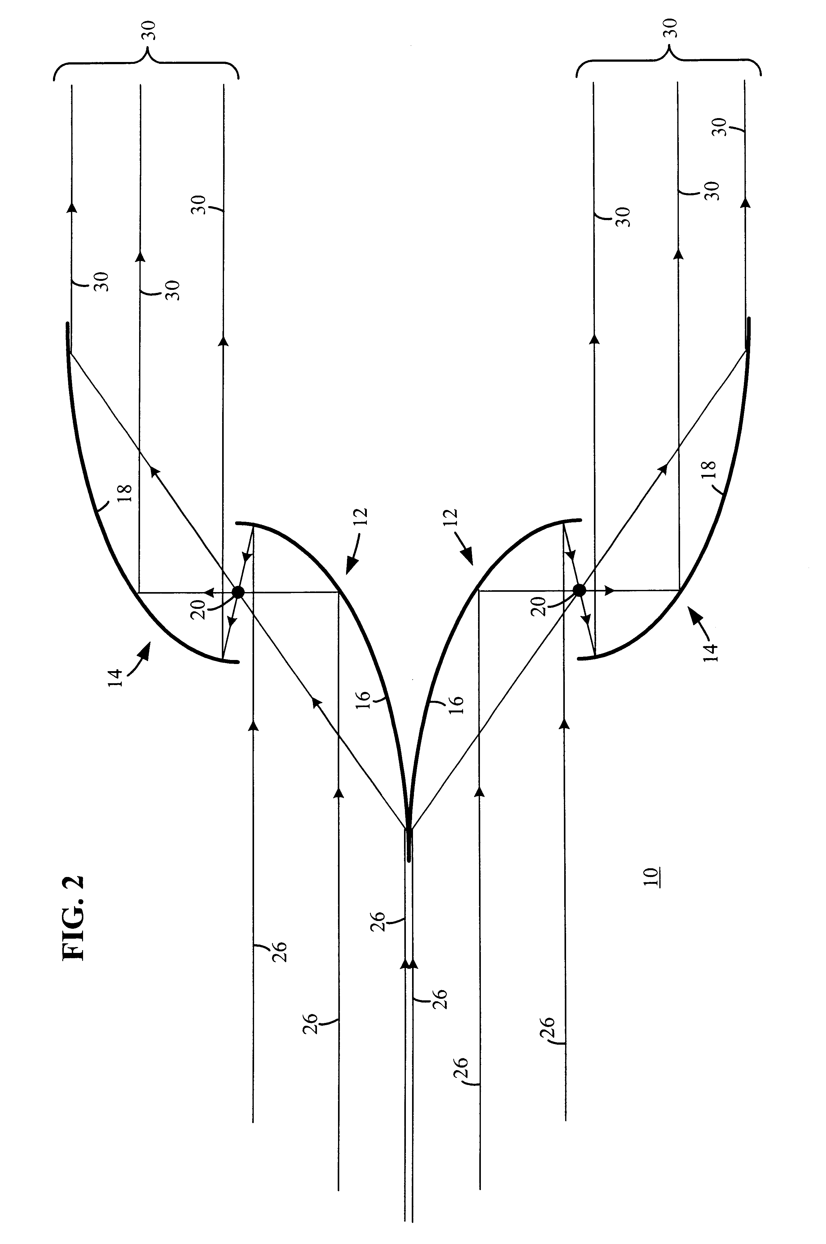
An example of a reflective illumination shaping device 10 is shown generally in FIG. 1. Although the illumination shaping device 10 is particularly well suited for off-axis step-and-scan microlithography, or the like, persons of ordinary skill in the art will readily appreciate that the teachings of the instant invention are not limited to any particular type of microlithography or microchip manufacturing illumination exposure process. On the contrary, the teachings of the invention can be employed with virtually any optical system where shaping the illumination pattern is desired. Thus, although the illumination shaping device 10 will be described below primarily in relation to off-axis lithographic microchip manufacturing using EUVL or deep ultraviolet lithography, persons of ordinary skill in the art will readily appreciate that the apparatus and method could likewise be used with any type of lithography methods, illumination system, exposure system, etc.

Generally, the illuminati...


PUM

PropertyMeasurementUnit
wavelengthsaaaaaaaaaa

Abstract

Methods and apparatuses for shaping an illumination pattern for off-axis lithography are disclosed. A disclosed apparatus includes a first and second reflecting objective. The first reflecting objective includes a first reflective surface that reflects input light having an on-axis illumination pattern through a first focal point. The second reflecting objective includes a second reflective surface that receives the reflected light through the first focal point and through a second focal point aligned with the first focal point, and reflects the reflected light through an output end as output light having an off-axis illumination pattern. A disclosed method includes receiving collimated light with a conventional illumination pattern centered on an optical axis, symmetrically reflecting the collimated light in multiple directions away from the optical axis and reflecting the reflected light to create output light having an off-axis illumination pattern symmetrical about the optical axis.

Description

FIELD OF THE TECHNOLOGYThe invention relates generally to lithography, and, more particularly, to deep ultraviolet and extreme ultraviolet lithographic exposure systems.DESCRIPTION OF THE PRIOR ARTIn microchip manufacturing, microlithography has been at the forefront of manufacturing techniques. Lithography is also generally the main factor that drives microchip technology and speed. As microchips require finer pattern structures in order to increase speed, the resolution of lithographic manufacturing techniques must keep pace. Many improvements in the lithographic process have involved utilizing illumination sources having shorter wavelengths to pattern the circuitry onto a substrate wafer. The shorter the wavelength of the illumination source, typically the better the resolution and quality of the circuit lines patterned onto the substrate wafer.One such lithographic process is deep ultraviolet lithography which is currently used for most microchip manufacture. Depending of the sp...

Claims


Application Information

Patent Timeline
Patent Type & Authority Patents(United States)
IPC IPC(8): G03F7/20
CPCG03F7/70108G03F7/702
Inventor DOROS, THEODORE G.
Owner INTEL CORP
Why Eureka
Try Eureka