Wafer level packaging of micro electromechanical device

a technology of micro electromechanical devices and packaging, applied in the direction of fluid speed measurement, instrumentation, and details of semiconductor/solid-state devices, can solve the problems of reducing yield, difficulty in overcoming difficulties, and broad application range of fabrication technology relevant to micro electromechanical devices

Inactive Publication Date: 2004-03-23
XIANGQUN SCI & TECH
View PDF1 Cites 66 Cited by
  • Summary
  • Abstract
  • Description
  • Claims
  • Application Information

AI Technical Summary

Benefits of technology

The primary object of the present invention is to propose a wafer level package of micro electromechanical devices so that damage of the micro electromechanical devices due to external forces in the packaging procedure can be avoided.
Another object of the present invention is to use a silicon wafer as a package base so that the whole package device not only has good evenness and keeps good contact with a chip, but also has better thermal conductance. Packaged modules will thus have good heat-radiating effect.

Problems solved by technology

Different from the conventional IC fabrication technology, the fabrication technology relevant to micro electromechanical devices is very broad and complex.
However, some difficulties must be overcome.
First, the flushing of cooling water during the dicing procedure and the small powders resulted from dicing will damage suspended devices so that the yield will be reduced.
Secondly, micro electromechanical devices will be fixed during the procedure of compound molding so that the object of enhancing their sensitivity by suspended structures will be lost.

Method used


Image

  • Wafer level packaging of micro electromechanical device
  • Wafer level packaging of micro electromechanical device
  • Wafer level packaging of micro electromechanical device

Examples


Embodiment Construction

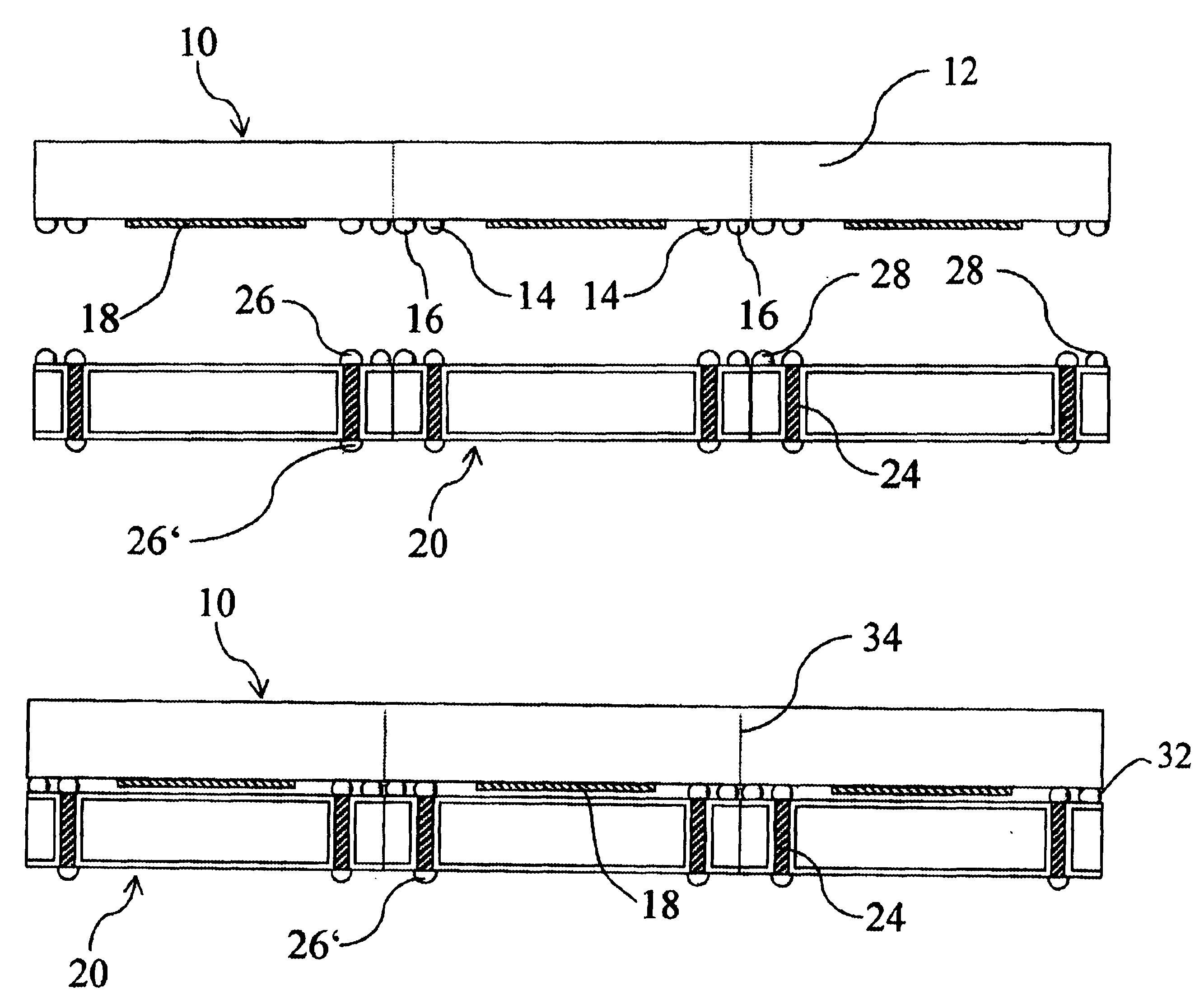
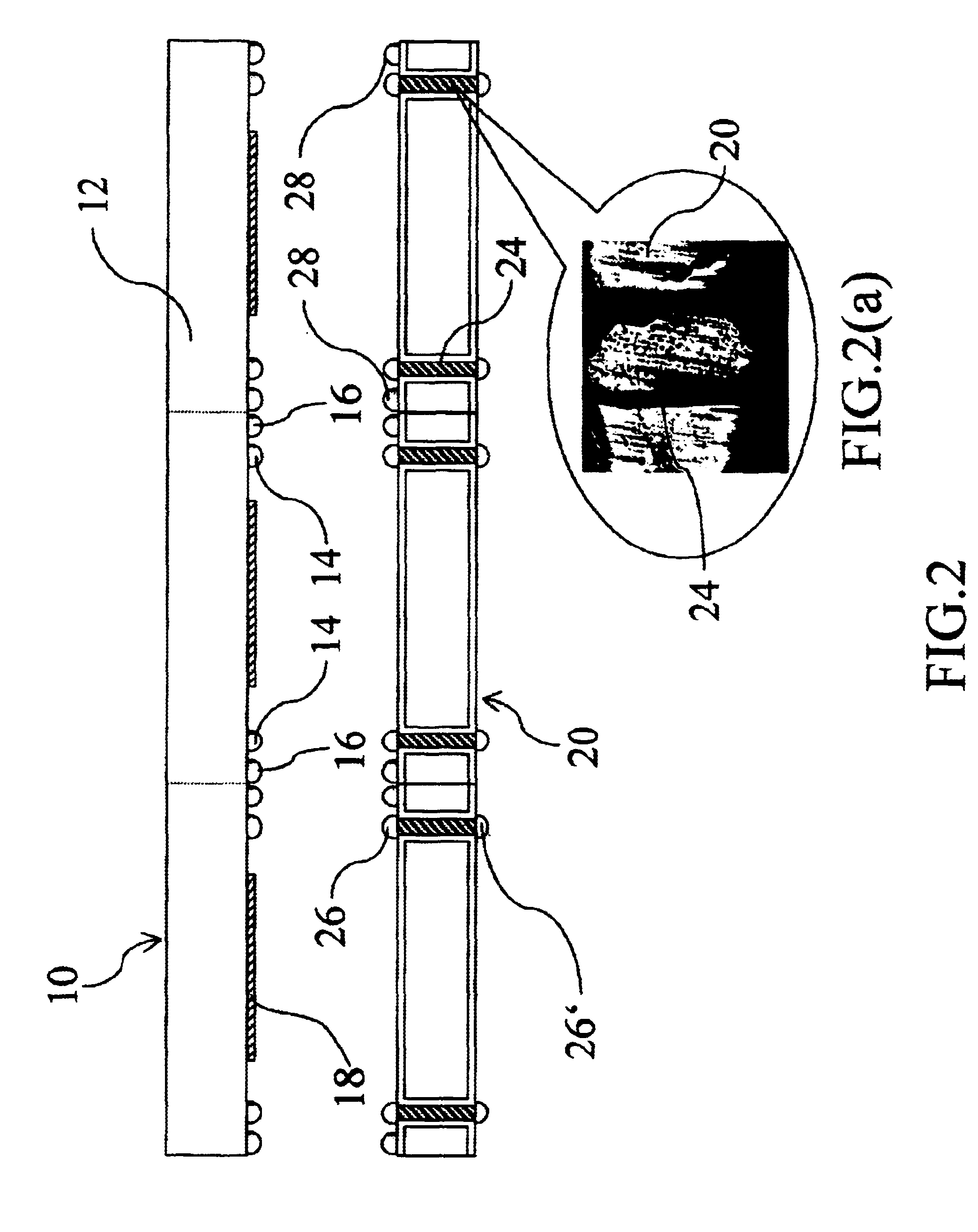
The present invention is characterized in that conductor plugs and bonding solders of a package wafer base are exploited to electrically connect I / O bonding pads of micro electromechanical devices to the exposed surface of the package wafer base. The other surface of the package wafer base is glued with the micro electromechanical device wafer to form a wafer level package, which is then diced into a plurality of single chip modules.

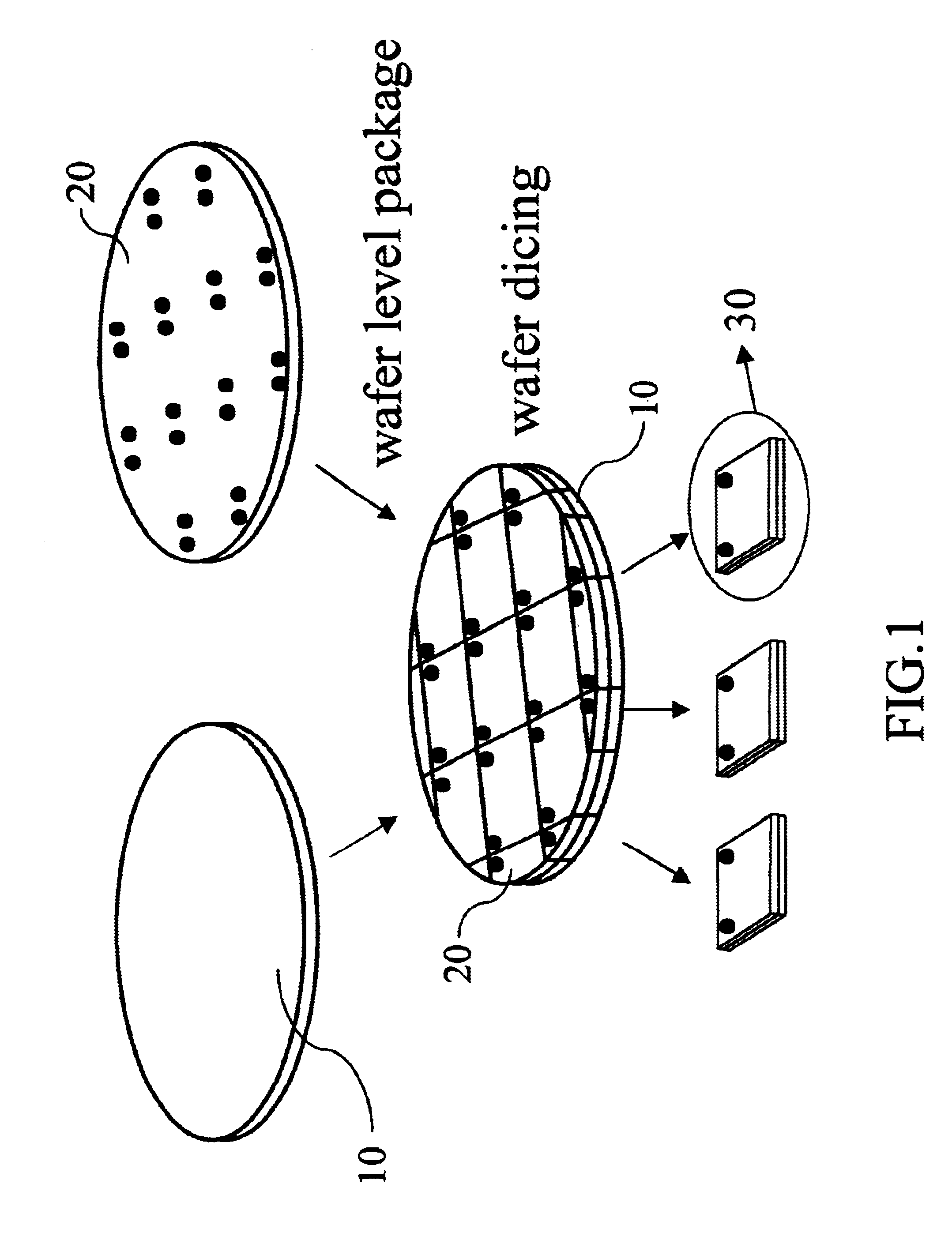
As shown in FIG. 1, a micro electromechanical device wafer 10 and a package silicon wafer 20 of the same size are glued with solders and are then diced into a plurality of single chip modules 30. The utmost advantage of this method is that damage to micro electromechanical devices due to external forces during the packaging procedure can be avoided. Moreover, better evenness can be obtained by using a silicon wafer as a package base as compared to other materials. Also, thermal expansion coefficients of the two wafers can be considered to be the same so ...


PUM

PropertyMeasurementUnit
depth/width aspect ratioaaaaaaaaaa
thicknessaaaaaaaaaa
widthaaaaaaaaaa

Abstract

The present invention provides a wafer level package of micro electromechanical devices. The wafer level package of the present invention comprises a wafer having a plurality of micro electromechanical devices and a package wafer of the same size. A plurality of conductor plugs penetrate through the upper and lower surfaces of the package wafer. Solder bumps are formed on the conductor plugs to be adhered to predetermined solder bumps on the micro electromechanical device wafer so as to form a package device. The wafer level package of the present invention can prevent micro electromechanical devices from damage during the packaging procedure.

Description

The present invention relates to a wafer level package technique and, more particularly, to a wafer level package structure of micro electromechanical devices.In the semiconductor industry, the micro-machining technology is a newly developing technique. It exploits the integrated-circuit (IC) technology to fabricate various kinds of micro-sensors and micro-drivers. Additionally, the micro-machining technology integrated with micro-electronic circuits can constitute micro-systems, which is called micro electromechanical system (MEMS).Different from the conventional IC fabrication technology, the fabrication technology relevant to micro electromechanical devices is very broad and complex. However, most micro electromechanical devices make use of the micro-machining technology to fabricate suspended structures having only a few supporting points so as to enhance mechanical sensitivity thereof (e.g., pressure sensors), or to reduce thermal conductance thereof (e.g., thermal sensors). In...

Claims


Application Information

Patent Timeline
Patent Type & Authority Patents(United States)
IPC IPC(8): B81B7/00B81C1/00H01L23/12H01L23/14H01L23/498
CPCB81B7/007B81C1/00888H01L23/147H01L23/49827H01L2224/16H01L2924/01079H01L2924/09701
Inventor CHOU, BRUCE C. S.WU, HSIEN-MINGSUN, PING-CHIN
Owner XIANGQUN SCI & TECH
Why Eureka
Try Eureka