Semiconductor switching element driving circuit

a switching element and driving circuit technology, applied in the direction of electronic switching, pulse technique, electrical apparatus, etc., can solve the problems of high current change rate, and inability to maintain malfunction withstand capacity,

Inactive Publication Date: 2004-04-06
DENSO CORP
View PDF24 Cites 110 Cited by
  • Summary
  • Abstract
  • Description
  • Claims
  • Application Information

AI Technical Summary

Benefits of technology

is preferably to prevent a semiconductor switching element from being destroyed due to an overcurrent caused by a short circuit and the like.
In this manner, when the second overcurrent (short circuit current) is caused by a load short circuit, an arm short circuit or the like, a voltage applied to a gate terminal is dropped instantaneously by the overcurrent limiting circuit so that the overcurrent can be prevented from flowing into the semiconductor switching element. Additionally, when the first overcurrent smaller than the short circuit current that is generated for a relatively long time is caused by a motor lock or the like, the overcurrent protection circuit first decreases the main current at the first inclination and then reduces the main current at the second inclination steeper than the first inclination, whereby the high-speed cutoff of the semiconductor switching element can be conducted while preventing the effect of the jumping voltage due to the wiring inductance. Therefore, the overcurrent which increases instantaneously can be controlled and the high-speed cutoff of the semiconductor switching element can be conducted.
For example, as shown in claim 2, the overcurrent limiting circuit may reduce the voltage of the gate terminal in the case that it becomes a larger current within a shorter period of time than a delay time in the circuit.
In this manner, when the main current has become larger than the first comparison current, the gate voltage can be dropped instantaneously by the overcurrent limiting circuit. In addition, the main current is decreased at the first inclination when the main current becomes larger than the second comparison current and the main current is reduced at the second inclination steeper than the first inclination when the main current becomes smaller than the third comparison current. Thus, the high-speed cutoff of the semiconductor switching element can be conducted while the effect of the jumping voltage due to the wiring inductance is prevented. Furthermore, regardless of a period of time after the overcurrent has occurred, the main current is suddenly dropped at the time when the main current has become smaller than the third comparison current so that the overcurrent can also be prevented from inevitably flowing through for a fixed time.
In this manner, until a control voltage (a gate voltage) reaches a predetermined resistance switching voltage value during current carrying through an electric load (i.e, semiconductor switching element), a detection resistance switching unit reduces the resistance value of the current detection resistance. Thus, a voltage drop by the current detection resistor whose resistance value has been reduced is inputted into an overcurrent protecting unit as a detected voltage. Therefore, in the case that the control voltage is low and a ratio of the detected voltage to the current carrying through the load is great (i.e., the current mirror ratio is small), the resistance value of the current detection resistor is decreased to allow a protecting operation not to be conducted with a small amount of the current carrying through the semiconductor switching element (the reduction in the control voltage by the overcurrent protecting unit).

Problems solved by technology

On this account, cutting off the IGBT at high speed while retaining a malfunction withstand capacity is difficult.
Additionally, when a gate voltage is cut off, a voltage is varied from a normal driving voltage to 0V at high speed and thus a rate of a current change -dI / dt at the high-speed cutoff becomes great, a jumping voltage caused by a wiring inductance is increased and the IGBT may be broken by an excess current caused by breakdown due to the jumping voltage larger than a withstand voltage.
On the other hand, when a motor lock or the like occurs, an overcurrent that is smaller than the short circuit current is generated for a relatively long time.
Thus, the flow of the short circuit current through the IGBT 101 cannot be prevented.
Furthermore, the short circuit current flowing at this time greatly increases in magnitude (five-fold or more of a rated current, for example) because an extremely large motor driving voltage.
Consequently, the IGBT might be damaged.
Additionally, since the conventional semiconductor switching element driving circuit cannot turn off the overcurrent until the delay time T1 passes, the overcurrent is also supplied to the other IGBTs shown in FIG. 12 and it causes a motor system to have a problem.

Method used


Image

  • Semiconductor switching element driving circuit
  • Semiconductor switching element driving circuit
  • Semiconductor switching element driving circuit

Examples


first embodiment

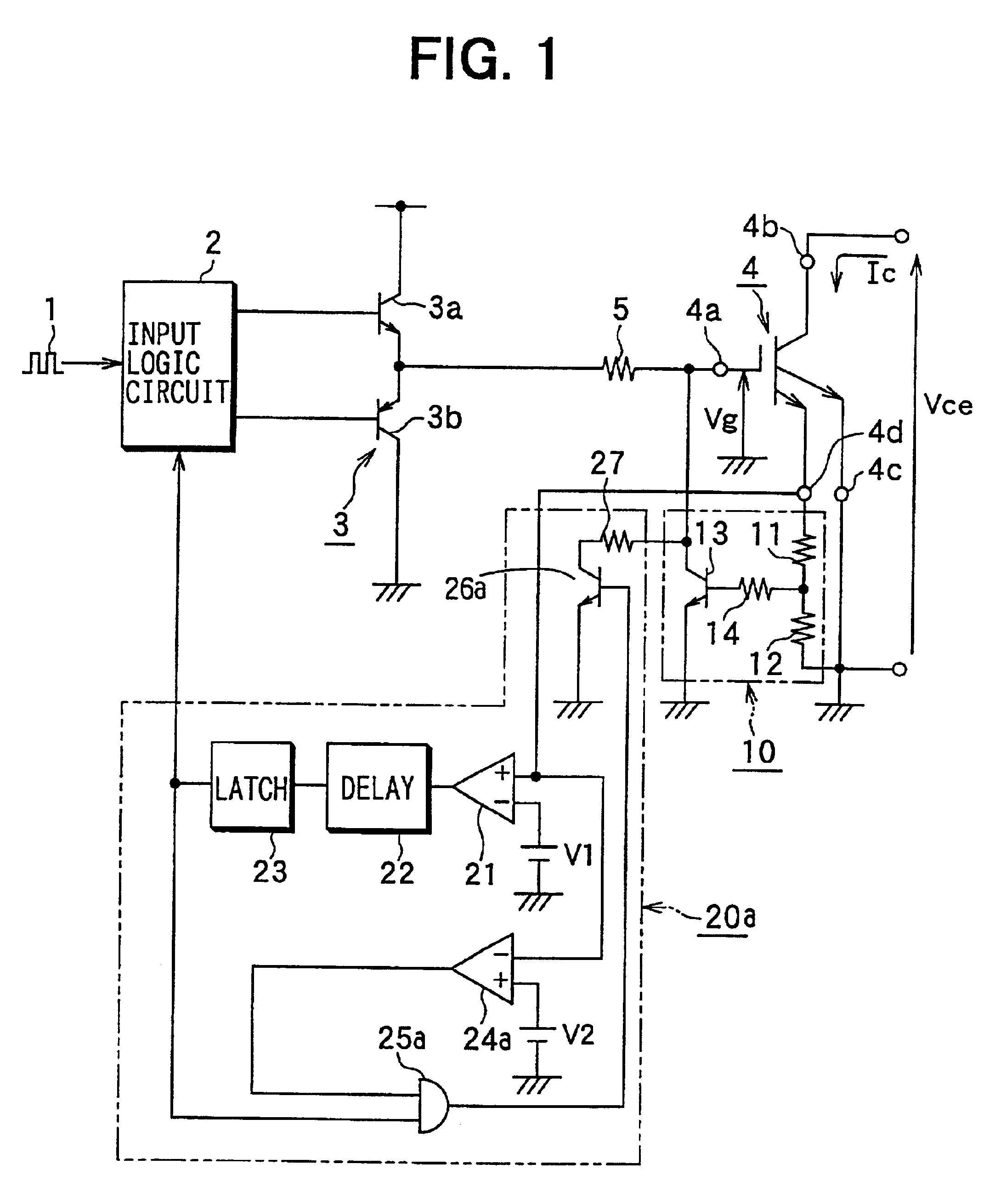
FIG. 1 illustrates a circuitry of a semiconductor switching element driving circuit to which a first embodiment of the invention is applied. This semiconductor switching element driving circuit is for use in driving each of semiconductor switching elements of a motor driving circuit of the electric vehicle or the like as shown in FIG. 12. Hereafter, the description of the semiconductor switching element driving circuit will be made according to FIG. 1.

The semiconductor switching element driving circuit shown in FIG. 1 comprises an input logic circuit 2 to which an input signal 1 such as a PWM signal or the like is inputted, a driver circuit 3 controlled by the input logic circuit 2 to turn it on / off, an IGBT 4 for performing switching in response to the turn on / off of the driver circuit 3, an overcurrent limiting circuit 10 for limiting a flow of an overcurrent (short circuit current) that flows to the IGBT 4 and becomes enormously large in a relatively short time, and an overcurren...

second embodiment

FIG. 3 illustrates a circuitry of a semiconductor switching element driving circuit in a second embodiment. The semiconductor switching element driving circuit in this embodiment is partially modified the circuitry with respect to the first embodiment and thus only different portions will be described.

As shown in FIG. 3, the semiconductor switching element driving circuit in this embodiment has different configuration of an overcurrent protection transistor 26b from the overcurrent protection transistor 26a shown in FIG. 1. That is, in a second comparator 24b, the gate voltage of an IGBT 4 is compared with a predetermined voltage V3. Moreover, a change in a decreasing ratio of the collector Ic is controlled by an overcurrent protection transistor 26b based on an output of this second comparator 24b. Namely, the comparator 24b serves as the comparator 24a in the first embodiment. It is noted that a circuit for turning off the transistor 26b after the IGBT 4 is cut off is not shown in...

third embodiment

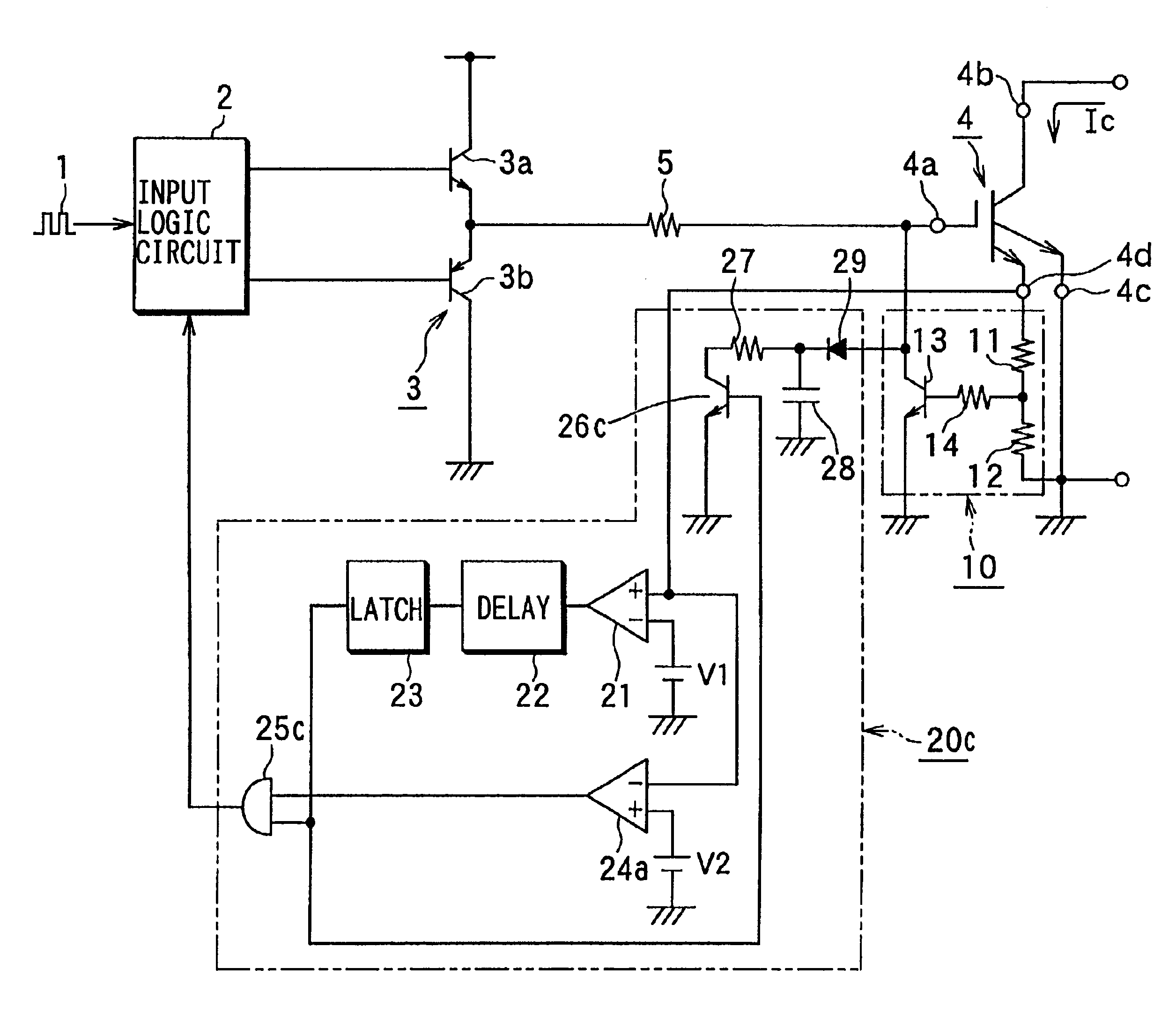
FIG. 4 illustrates a circuitry of a semiconductor switching element driving circuit in a third embodiment. The semiconductor switching element driving circuit in this embodiment is partially modified the circuitry with respect to the first embodiment and thus only different portions will be described.

As shown in FIG. 4, a turning on / off of an overcurrent protection transistor 26c is controlled according to an output signal of a latch circuit 23. Additionally, the input logic circuit 2 controls turning on / off of a driver circuit 3 based on an output of an AND circuit 25c to which output signals of the latch circuit 23 and the second comparator 24a are inputted.

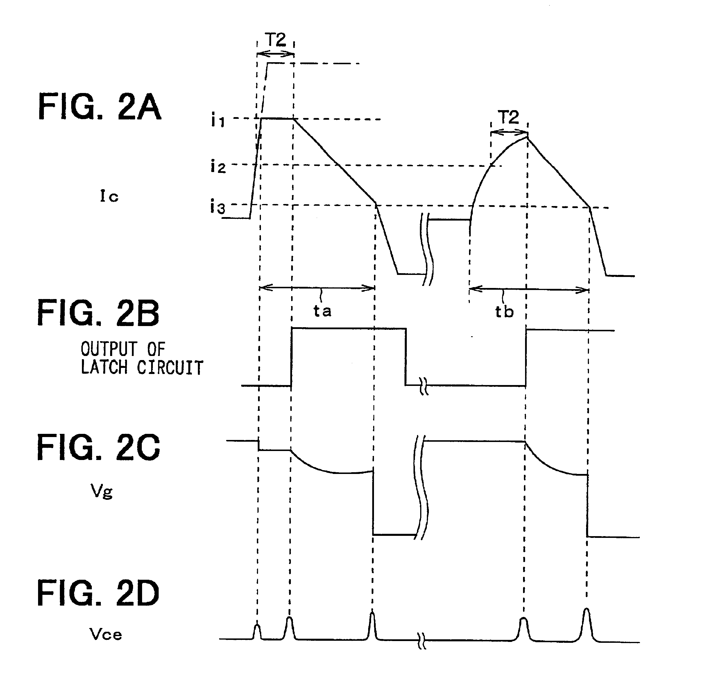
Therefore, when the overcurrent is about to occur for a relatively long time, the overcurrent protection transistor 26c is turned on to decrease the collector current at the first inclination as shown in FIG. 2 and subsequently the sink driver 3b of the driver circuit 3 is turned on to decrease the collector current at the seco...


PUM


Abstract

A semiconductor switching element driving circuit comprises an overcurrent limiting circuit which instantaneously drops a voltage of a gate terminal of an IGBT when a main IGBT current becomes larger than a predetermined level i1. An overcurrent protection circuit which first decreases the main IGBT current at a first inclination when the main IGBT current becomes larger than the other level i2 lower than the i1 and then reduces the main IGBT current at a steep second inclination when it becomes smaller than another level i3.

Description

This application is based on Japanese Patent Application Nos. 2000-101305 filed on Mar. 31, 2000, 2000-232985 filed on Aug. 1, 2000, and 2001-27323, filed on Feb. 2, 2001, the contents of which are incorporated herein by reference.1. Field of the InventionThe present invention relates to a semiconductor switching element driving circuit having an overcurrent protection function, in particular, which is preferably applied to a circuit for driving an IGBT or the like that is used in a motor driving circuit of an electric vehicle or the like.2. Related ArtsIn the case of using a semiconductor switching element, e.g. the IGBT for driving a motor, when a load short circuit or the like occurs, a collector current of the IGBT rapidly increases and the IGBT is broken by an overcurrent or heat. Therefore, in order to prevent the IGBT from being destroyed, there is a need to detect the overcurrent to cut off the IGBT by a protection circuit within a short time.However, since there is a case w...

Claims


Application Information

Patent Timeline
Patent Type & Authority Patents(United States)
IPC IPC(8): H03K17/16H03K17/082
CPCH03K17/0828H03K17/168
Inventor FUKUDA, YUTAKAOKUDA, RYOICHIMAKINO, TOMOATSUYAGI, KENJITSUZUKI, YUKIO
Owner DENSO CORP
Why Eureka
Try Eureka