Method for prediction random defect yields of integrated circuits with accuracy and computation time controls

a technology of random defect and computation time control, which is applied in the direction of measurement devices, semiconductor/solid-state device testing/measurement, instruments, etc., can solve problems such as excessive computer resource expenditure on problems, failures, and inability to accurately predict random defect yields of integrated circuits

Inactive Publication Date: 2004-05-18
GOOGLE LLC
View PDF22 Cites 100 Cited by
  • Summary
  • Abstract
  • Description
  • Claims
  • Application Information

AI Technical Summary

Problems solved by technology

Some of these defects will cause electrical failures (faults), and similar electrical failures are collectively referred to as a failure mechanism.
Since it is not practical to calculate a probability of failure for every possible defect size, the defect size distribution must be approximated, introducing error into the larger problem of projecting electrical test yield.
The result is a yield estimate in which the error is not clearly understood, and there was likely an excessive amount of computer resource spent on the problem.
For a fabricator making multiple ICs, the problem quickly becomes self-limiting.

Method used


Image

  • Method for prediction random defect yields of integrated circuits with accuracy and computation time controls
  • Method for prediction random defect yields of integrated circuits with accuracy and computation time controls
  • Method for prediction random defect yields of integrated circuits with accuracy and computation time controls

Examples


Embodiment Construction

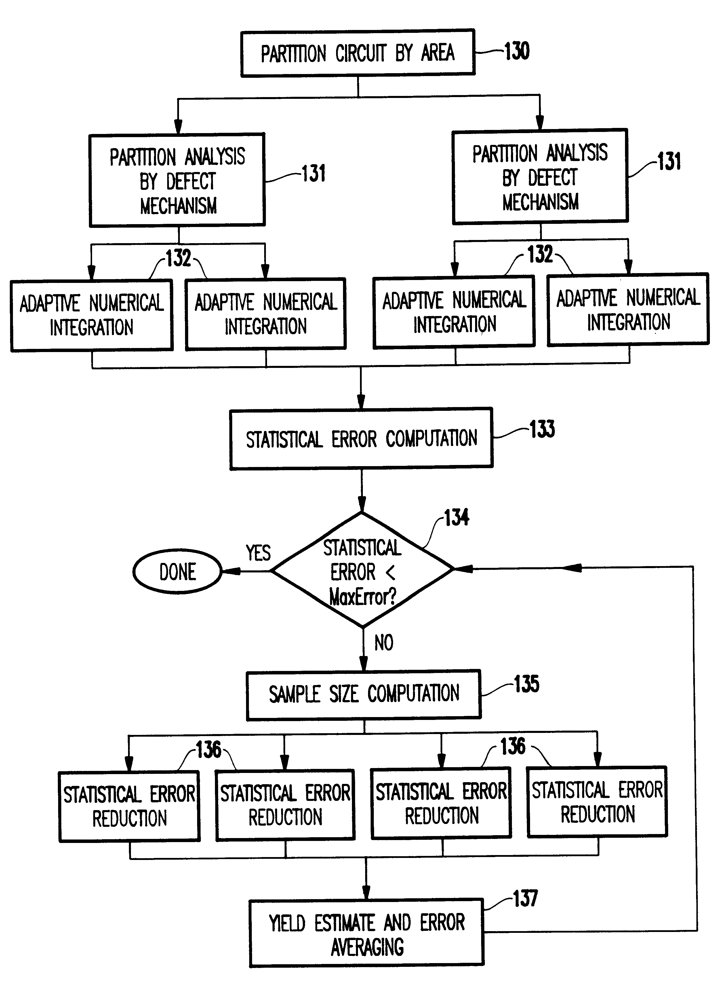
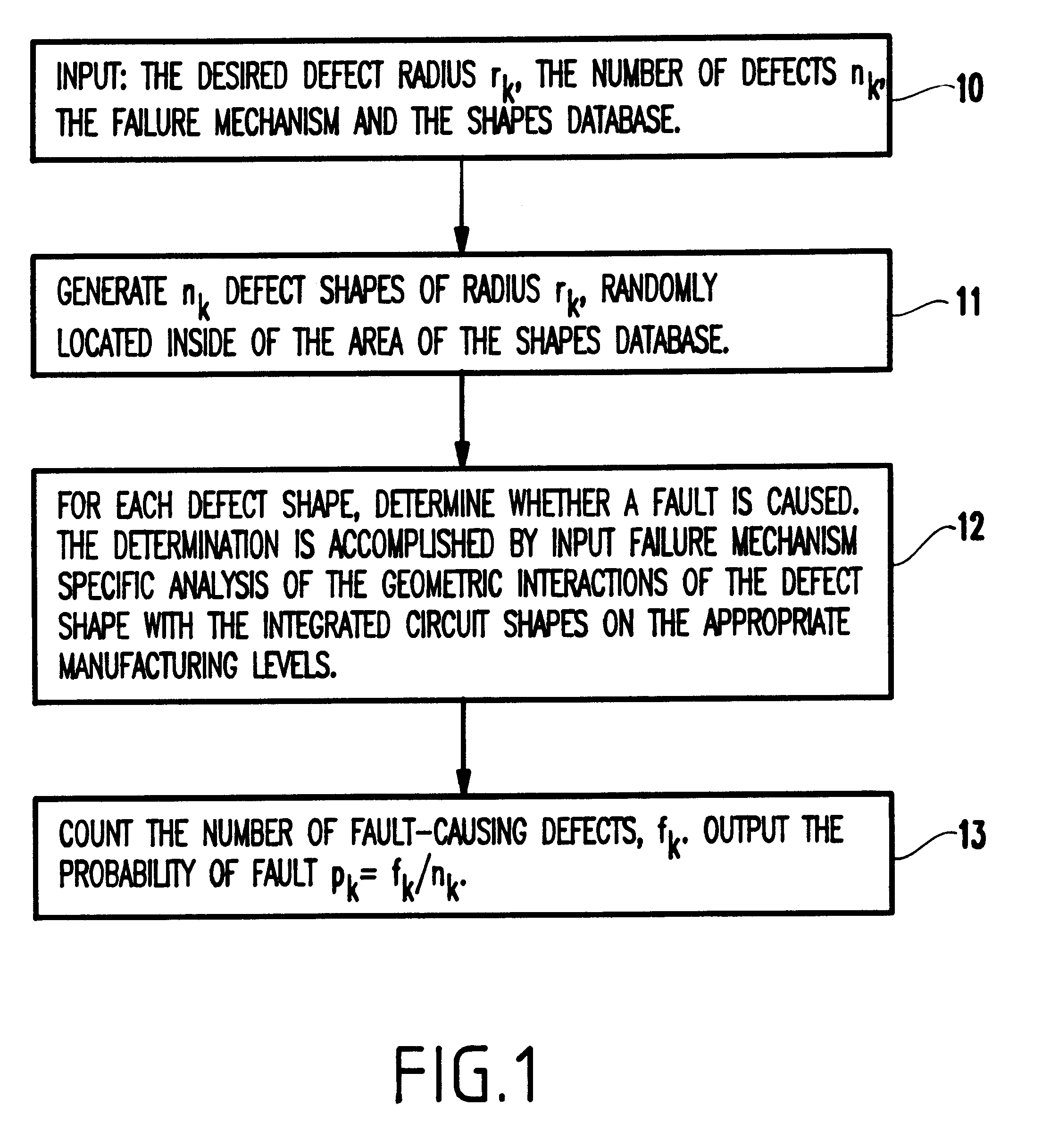
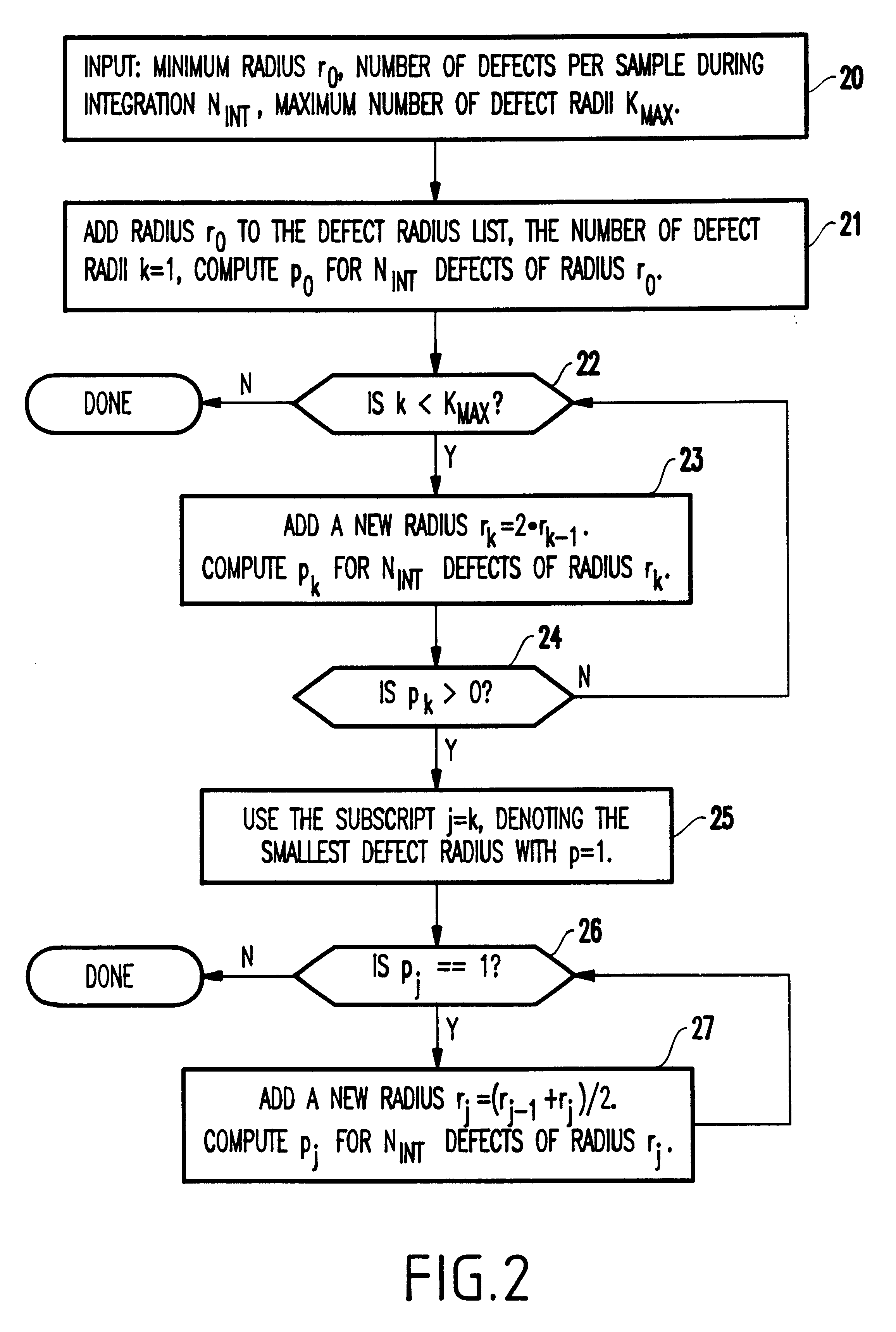
The electrical test yield of an IC may be predicted using a computer modeling program prior to the actual physical production. Such conventional modeling programs assess the circuit layout sensitivity to unintended opens or shorts, which may be the result of foreign material present in a clean room manufacturing environment.

In this application such particles of foreign matter on the surface of a wafer are referred to as defects, and those defects causing the circuit to operate in an unintended manner (electrical failure) are faults. The invention classifies faults into different defect mechanisms. Interacting defect mechanisms are collectively referred to as a failure mechanism. For example, a single layer of patterned metal wiring (metal 1) could have two failure mechanisms, one being a metal 1 open failure mechanism and the other being a metal 1 short failure mechanism. Each of these failure mechanisms would be made up of one or more defect mechanisms. Therefore, the metal 1 short...


PUM


Abstract

A method of computing a manufacturing yield of an integrated circuit having device shapes includes sub-dividing the integrated circuit into failure mechanism subdivisions (each of the failure mechanism subdivisions includes one or more failure mechanism and each of the failure mechanisms includes one or more defect mechanisms), partitioning the failure mechanism subdivisions by area into partitions, pre-processing the device shapes in each partition, computing an initial average number of faults for each of the failure mechanisms and for each partition by numerical integration of an average probability of failure of each failure mechanism, (the numerical integration produces a list of defect sizes for each defect mechanism, and the computing of the initial average includes setting a maximum integration error limit, a maximum sample size for a population of each defect size, and a maximum number of allowable faults for each failure mechansim), and computing a final average number of faults for the integrated circuit by iterativelly reducing a statistical error of the initial average number of faults for each of the failure mechanisms until the statistical error is below an error limit.

Description

1. Field of the InventionThis invention generally relates to the prediction of electrical test yield for semiconductor integrated circuits (IC), or of electronic packages, and the influence of design and process characteristics upon those tests; more particularly, to an efficient procedure for the prediction of random defect yields which are practical for large chips.2. Description of the Related ArtElectrical test yield is the most variable productivity component from product to product, and through the evolution and development of a process technology. Electrical test yield, Y, is defined as the product of systematic (gross) yield, Y.sub.0, and random defect yield (usually the dominant component), Y.sub.R. Defects may be randomly introduced during the various steps of IC fabrication. Some of these defects will cause electrical failures (faults), and similar electrical failures are collectively referred to as a failure mechanism. The random defect yield is a function of average num...

Claims


Application Information

Patent Timeline
Patent Type & Authority Patents(United States)
IPC IPC(8): G01R31/28G01R31/317H01L21/66
CPCG01R31/31705H01L22/20
Inventor ALLEN, ARCHIBALD J.DONATH, WILM E.DZIEDZIC, ALAN D.LAVIN, MARK A.MAYNARD, DANIEL N.NEWNS, DENNIS M.TELLEZ, GUSTAVO E.
Owner GOOGLE LLC
Why Eureka
Try Eureka