Semiconductor device downsizing its built-in driver

a technology of built-in drivers and semiconductors, applied in the field of semiconductor devices, can solve the problems of affecting the optimization of mcp products, increasing current consumption by that amount, and limited countermeasures against noise generation and current consumption at the operation

Inactive Publication Date: 2004-06-29
RENESAS ELECTRONICS CORP
View PDF4 Cites 11 Cited by
  • Summary
  • Abstract
  • Description
  • Claims
  • Application Information

AI Technical Summary

Benefits of technology

As described above, the present embodiment 5 is configured such that the chip 1012 includes the first pad 111 to be connected to the another semiconductor device installed in the MCP; the second pad 112 for making the probing connection in the wafer test; the first buffer 450 for driving the another semiconductor device to be connected to the first pad 111; and the second buffer 460, being driven by the first buffer 450, drives the load capacitance of the tester connected to the second pad 112 by the driving power greater than that of the first buffer 450, and has its active / inactive state controlled in response to the control signal 150. Thus, the present embodiment 5 drives the another semiconductor device by the first buffer 450 with the smaller driving power after the assembly, whereas it drives the load capacitance of the tester by the second buffer 460 with the greater driving power in the wafer test. As a result, the present embodiment 5 offers an advantage of being able to prevent the noise generation and to limit the increase in the current consumption during the operation. Furthermore, connecting the control signal 150 of the second buffer 460 to the pad 114 facilitates the external control of the active / inactive state of the second buffer 460.

Problems solved by technology

This offers a problem of increasing the current consumption by that amount.
Second, as for the semiconductor devices to be installed in the MCP, and a structure provided for driving the another semiconductor device in the conventional technique to implement the MCP, the following problem arises.
For this reason, countermeasures against the noise generation and current consumption at the operation are limited, which hinders the optimization of the MCP product.

Method used


Image

  • Semiconductor device downsizing its built-in driver
  • Semiconductor device downsizing its built-in driver
  • Semiconductor device downsizing its built-in driver

Examples


embodiment 1

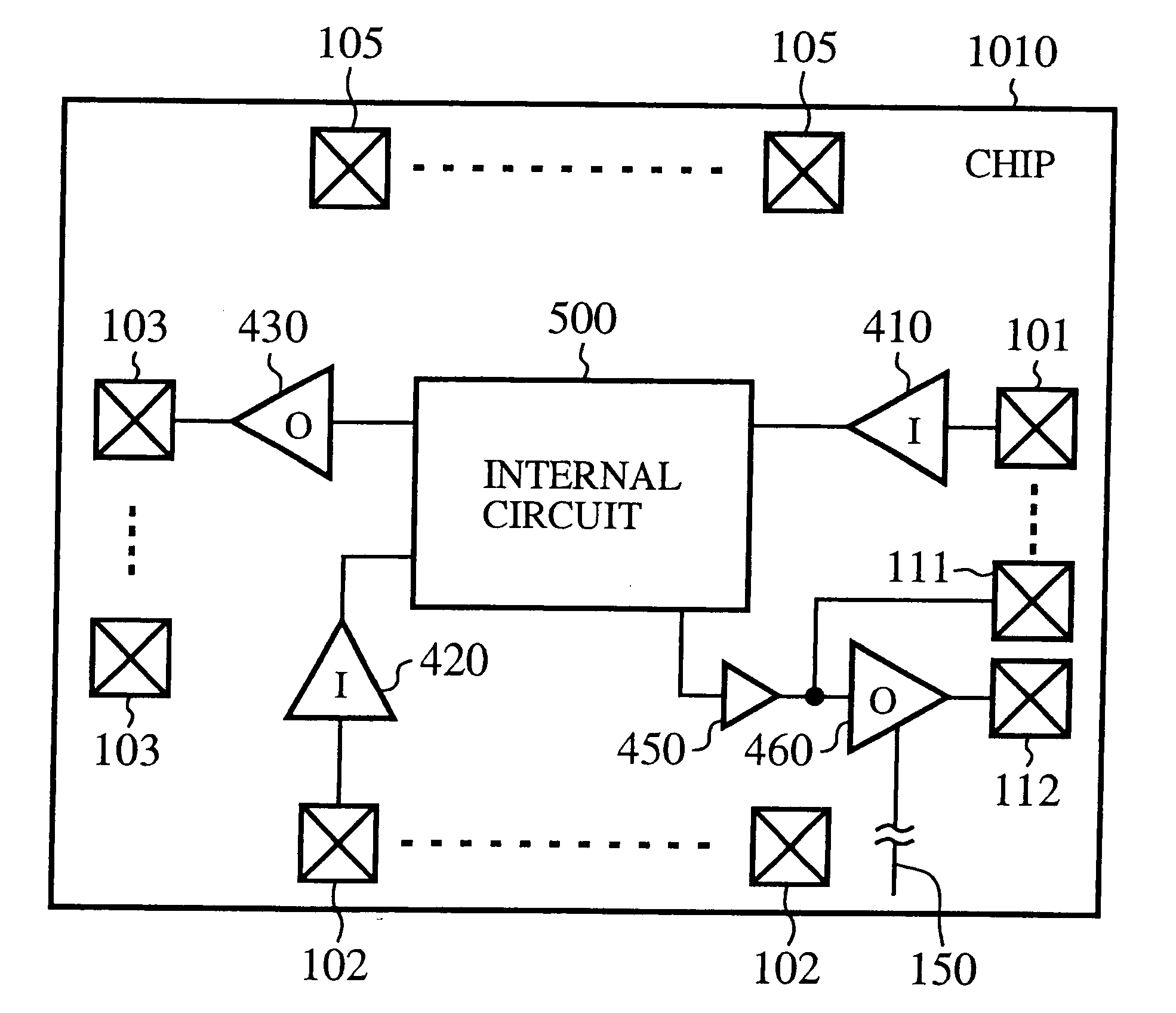
FIG. 1 is a block diagram showing a schematic configuration of a chip (semiconductor device) to be installed in a multi-chip package of an embodiment 1 in accordance with the present invention. In FIG. 1, the reference numeral 1010 designates a chip (semiconductor device). In the chip 1010, the reference numeral 500 designates an internal circuit, reference numerals 410 and 420 each designate an input buffer for the internal circuit 500, and the reference numeral 430 designates an output buffer. Reference numerals 101-103 designate pads that are formed on the chip, and connected to the input terminals of the input buffers 410 and 420, and to the output terminal of the output buffer 430. Reference numerals 105 each designate a pad for another input or output of the internal circuit 500 (not shown for the sake of simplicity).

The chip 1010 is a first semiconductor device to be incorporated into the MCP. It has a first pad 111 to be connected to an another semiconductor device (not show...

embodiment 2

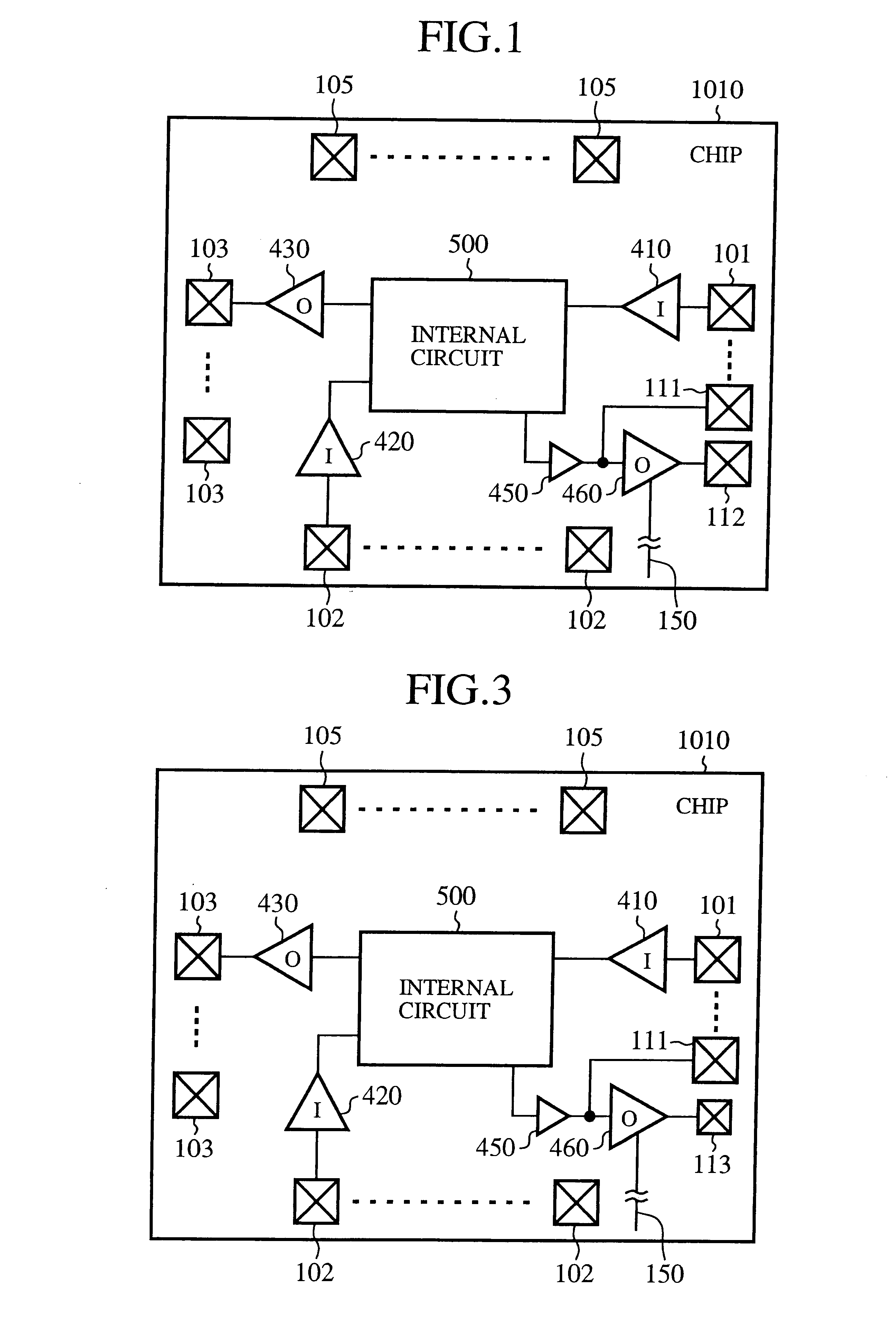
FIG. 3 is a block diagram showing a schematic configuration of a chip (semiconductor device) to be installed in the multi-chip package of an embodiment 2 in accordance with the present invention. In a chip 1011 as shown in FIG. 3, the reference numeral 500 designates an internal circuit, reference numerals 410 and 420 each designate an input buffer for the internal circuit 500, and the reference numeral 430 designates an output buffer. Reference numerals 101-103 designate pads that are formed on the chip, and connected to the input terminals of the input buffers 410 and 420 and to the output terminal of the output buffer 430. Each reference numeral 105 designates a pad for another input / output of the internal circuit 500 (not shown for the sake of simplicity).

The chip 1011 is a first semiconductor device to be incorporated into the MCP. It has a first pad 111 to be connected to an another semiconductor device and a second pad 113 for making a probing connection for a wafer test. The...

embodiment 3

FIG. 4 is a block diagram showing a schematic internal configuration of a multi-chip package of an embodiment 3 in accordance with the present invention. In FIG. 4, the reference numeral 1000 designates an MCP, and reference numerals 1010 and 1020 each designate a semiconductor device incorporated into the MCP 1000. Although the two semiconductor devices usually consist of chips with different types of functions, they may be chips of the same type. In either case, the MCP has a multi-chip structure for supplying data from a first chip to a second chip, or for exchanging data between them. The chips 1010 and 1020 built in the MCP 1000, which employs the multi-chip structure to exchange data between the two chips, have the different types of functions, and correspond to the chip described above in the embodiment 1.

In the chip 1010, the reference numeral 500 designates an internal circuit, reference numerals 410 and 420 each designate an input buffer for the internal circuit 500, and t...


PUM


Abstract

A semiconductor device includes a first pad, a second pad, a first buffer and a second buffer. The first pad is connected to another semiconductor device in a multi-chip package, and the second pad makes a probing connection in a wafer test. The first buffer drives the another semiconductor device connected to the first pad. The second buffer, being driven by the first buffer, drives a load capacitance of a tester connected to the second pad with the driving power greater than the driving power of the first buffer, and has its active / inactive state controlled by a control signal. The semiconductor device can provide the driving power necessary for the wafer test, and drive the another semiconductor device with preventing generation of drive noise and suppressing current consumption in the normal operation of the multi-chip package.

Description

1. Field of the InventionThe present invention relates to a semiconductor package that mounts a plurality of semiconductor chips in combination, and merges them by installing wiring between the chips to exchange data, that is, to a semiconductor device assembled in a multi-chip package.2. Description of Related ArtRecently, an increasing number of multi-chip packages (called "MCPs"from now on) have been used in electronic equipment such as mobile phones requiring miniaturization and versatility, as semiconductor products meeting demands of equipment manufacturers. The MCP consists of one package including combinations of LSIs such as logic and memory, digital and analog, and flash memory and SRAM LSIs, which are stacked and have wiring installed between the chips by wire bonding.FIG. 13 is a block diagram showing a schematic internal configuration of a conventional multi-chip package including two-chips (semiconductor devices) combined together. In FIG. 13, the reference numeral 110...

Claims


Application Information

Patent Timeline
Patent Type & Authority Patents(United States)
IPC IPC(8): G01R31/28H01L23/48H01L21/66H01L21/82H01L21/822H01L27/04
CPCG01R31/2884H01L2924/3011H01L2224/48091H01L2224/49175H01L2224/48137H01L2924/00014H01L2924/00H01L2224/05554H01L23/48
Inventor MIURA, MANABUHATAKENAKA, MAKOTOYAMASHITA, TAKEKAZU
Owner RENESAS ELECTRONICS CORP
Why Eureka
Try Eureka