
Light emitting device, display device and electronic instrument

a technology of light emitting devices and display devices, applied in the direction of electroluminescent light sources, organic semiconductor devices, electric lighting sources, etc., can solve the problem that the light emitted cannot be utilized at high efficiency, and achieve the effect of superior wavelength selectivity of light and efficient utilization of ligh

Inactive Publication Date: 2004-09-14
ELEMENT CAPITAL COMMERCIAL CO PTE LTD
View PDF20 Cites 1 Cited by
  • Summary
  • Abstract
  • Description
  • Claims
  • Application Information

AI Technical Summary

Benefits of technology

The present invention may provide a light emitting device that is superior in wavelength selectivity of light to be emitted in a direction intersecting a substrate and capable of efficiently utilizing light.
The first and second dielectric multi-layered films of this light emitting device enables to improve the wavelength selectivity. As a result, the light generated in the light-emitting layer by electro-luminescence emits at high efficiency in a narrow wavelength band corresponding to a high reflectance band of the first and second dielectric multi-layered films. In addition, since the electrode is disposed to avoid overlap with the light-emitting region in the light-emitting layer as viewed from the light emitting direction, absorption or scattering of light due to the electrode can be reduced. Therefore, the light generated in the light-emitting layer can be utilized at high efficiency.
(C) The light emitting device may further comprise: a third electrode disposed to interpose an insulating layer between the first electrode and the third electrode; and a fourth electrode disposed to interpose another insulating layer between the second electrode and the fourth electrode. The third and fourth electrodes may have a function as a gate for the first and second electrodes. For example, by applying a predetermined voltage to the third and fourth electrodes, the electron transport layer and the hole transport layer can be made to have different potentials, resulting that a lot of electrons in the electronic transport layer and a lot of holes in the hole transport layer can be moved into the light-emitting layer. Thus, the number of the electrons and holes contributing to light emission in the light-emitting layer can be increased, and the light emission efficiency can be raised.

Problems solved by technology

In an EL light emitting element using EL, isotropic light emission deteriorates the directivity so that the intensity of a light in a specific direction is low, and the emitted light cannot be utilized at high efficiency.

Method used


Image

  • Light emitting device, display device and electronic instrument
  • Light emitting device, display device and electronic instrument
  • Light emitting device, display device and electronic instrument

Examples


first embodiment

1. First Embodiment

1.1 Device Structure

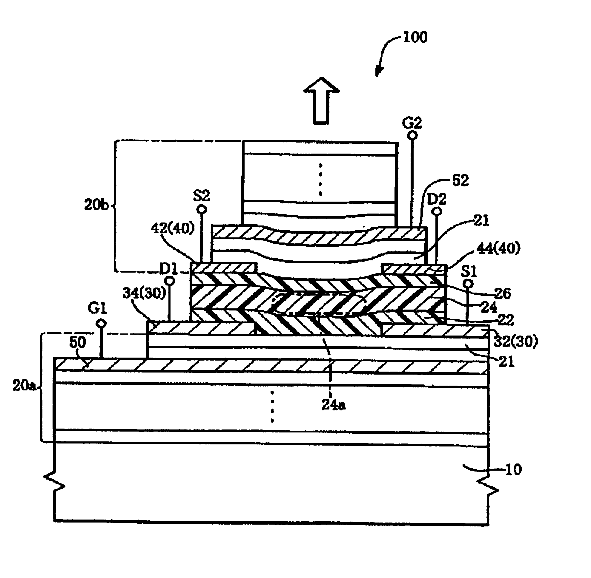
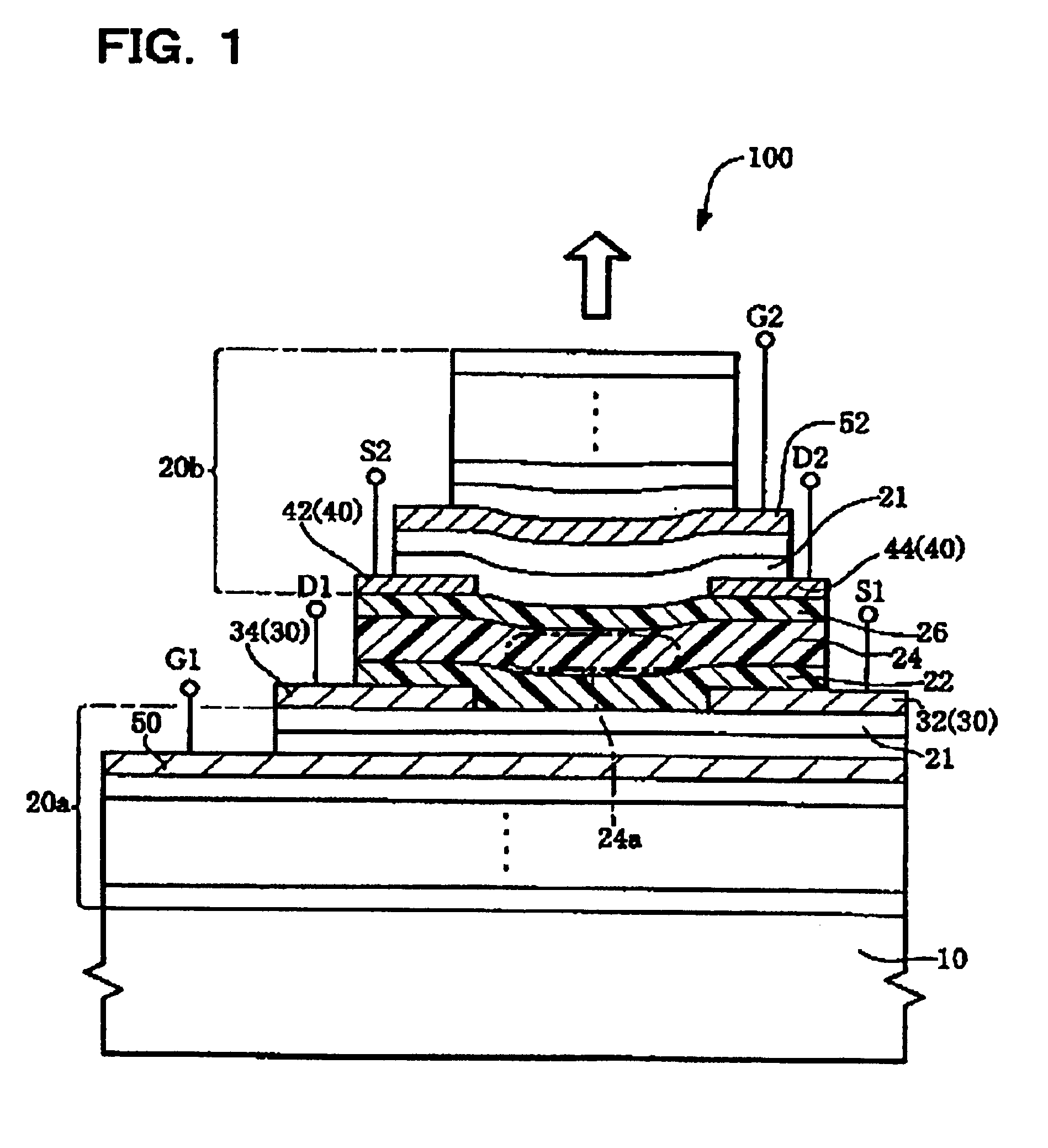
FIG. 1 is a cross-sectional view schematically showing a light emitting device 100 according to the first embodiment of the present invention.

The light emitting device 100 includes a light-emitting section on a substrate 10. The light-emitting section comprises a first dielectric multi-layered film 20a, an electron transport layer 22, a light-emitting layer 24, a hole transport layer 26 and a second dielectric multi-layered film 20b, which are piled in order.

The first dielectric multi-layered film 20a is provided thereon with a first electrode 30 consisting of a pair of electrode layers 32 and 34 for applying electrons to the electron transport layer 22. In this embodiment, one electrode layer 32 works as a source (S1) and the other electrode layer 34 works as a drain (D1). The electrode layers 32 and 34 are spaced each other, so that electrons are applied to the electron transport layer 22 by applying a predetermined voltage to the electrodes ...

second embodiment

2. Second Embodiment

2.1 Device Structure

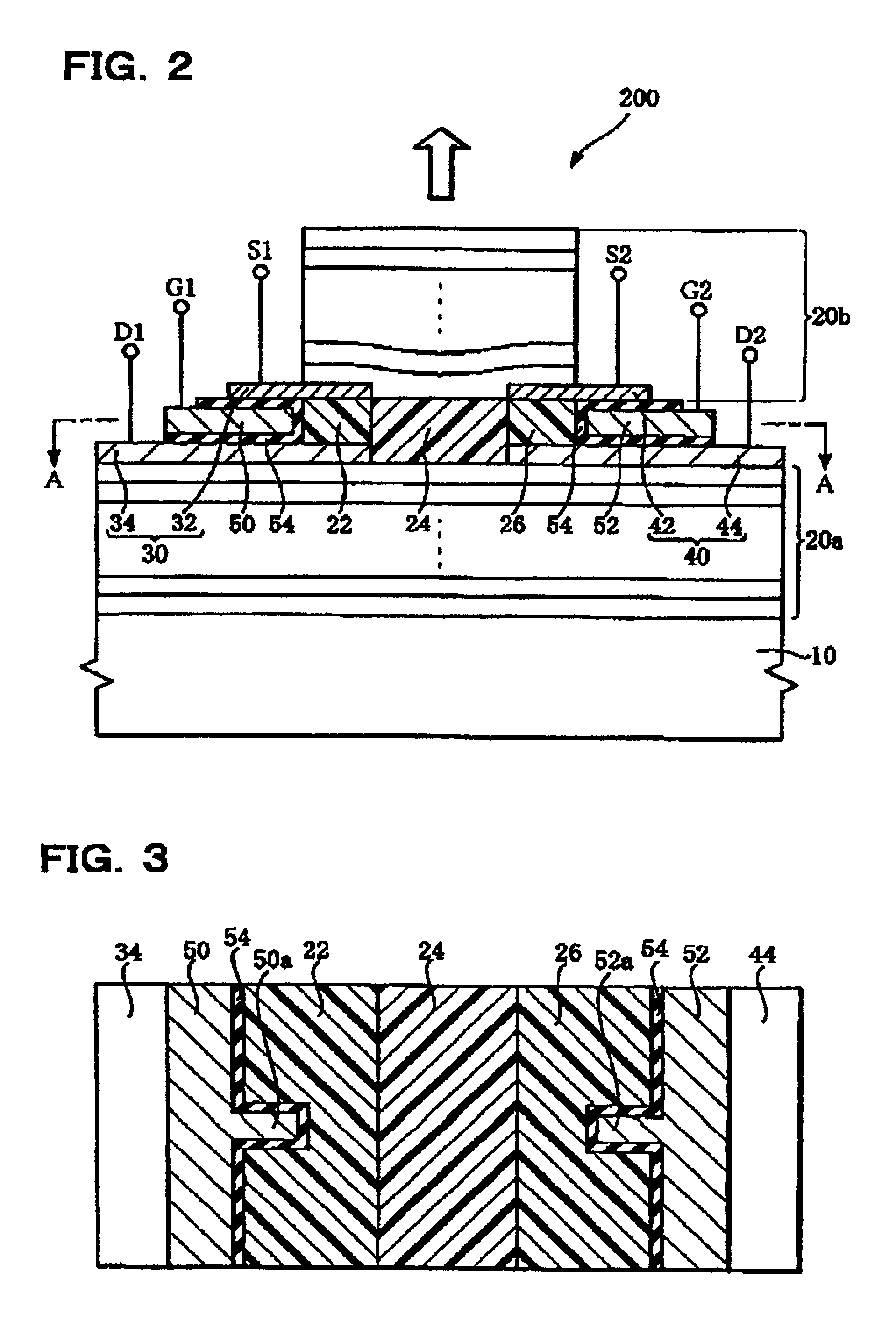
FIG. 2 is a cross-sectional view showing a light emitting device 200 according to the second embodiment of the present invention. FIG. 3 is a sectional view taken along the line A--A of FIG. 2, showing a main component. Disposition of the electron transport layer, the light-emitting layer and the hole transport layer is different from that of the first embodiment. The description below mainly concentrates on the differences between the first and second embodiments, and components having substantially the same functions as the components of FIG. 1 are denoted by the same reference numbers.

The light emitting device 200 includes a light-emitting section on a substrate 10. The light-emitting section comprises a first dielectric multi-layered film 20a, a light-emitting layer 24 and a second dielectric multi-layered film 20b, which are piled in order. In a direction parallel to a surface of the substrate 10, provided is an electron transport layer 2...

third embodiment

3. Third Embodiment

3.1 Device Structure

FIG. 5 is a cross-sectional view schematically showing a light emitting device 300 according to the third embodiment of the present invention. The structure of the first and second electrodes in this embodiment is different from those of the first and second embodiments. The description below mainly concentrates on the differences between the first and second embodiments and the third embodiment, and components having substantially the same functions as the components of FIG. 1 are denoted by the same reference numbers.

The light emitting device 300 includes a light-emitting section on a substrate 10. The light-emitting section comprises a first dielectric multi-layered film 20a, an electron transport layer 22, a light-emitting layer 24, a hole transport layer 26 and a second dielectric multi-layered film 20b, which are piled in order.

The first dielectric multi-layered film 20a is provided thereon with a cathode 60 connected to the electrode tra...


PUM


Abstract

A light emitting device has a substrate and a light-emitting section formed on the substrate. The light-emitting section includes a light-emitting layer in which light is generated by electro-luminescence, first and second electrodes used to apply electric charges to the light-emitting layer, and first and second dielectric multi-layered films between which the light-emitting layer is interposed. The first and second electrodes are disposed to avoid overlap with a light-emitting region in the light-emitting layer as viewed from a light emitting direction.

Description

Japanese Patent Application No. 2001-66612, filed on Mar. 9, 2001, and Japanese Patent Application No. 2002-60135 filed on Mar. 6, 2002 are herein incorporated by reference in their entirety.BACKGROUND OF THE INVENTIONThe present invention relates to a surface-emitting type of light emitting device using electro-luminescence (EL), and a display device and an electronic instrument using the light emitting device.In an EL light emitting element using EL, isotropic light emission deteriorates the directivity so that the intensity of a light in a specific direction is low, and the emitted light cannot be utilized at high efficiency.BRIEF SUMMARY OF THE INVENTIONThe present invention may provide a light emitting device that is superior in wavelength selectivity of light to be emitted in a direction intersecting a substrate and capable of efficiently utilizing light.The present invention may also provide a display device and an electronic instrument using the light emitting device.Accordi...

Claims


Application Information

Patent Timeline
Patent Type & Authority Patents(United States)
IPC IPC(8): H01L51/50H01L51/52H05B33/26H05B33/02H05B33/24
CPCH01L51/5203H01L51/5265H01L2251/5315H10K50/30H10K2102/3026H10K59/805H10K59/876H10K50/852H10K50/805
Inventor KOYAMA, TOMOKOKANEKO, TAKEO
Owner ELEMENT CAPITAL COMMERCIAL CO PTE LTD
Learn More