

Multilayer circuit board and method of manufacturing the same
a multi-layer circuit board and manufacturing method technology, applied in the direction of conductive material removal by irradiation, printed circuit non-printed electric component association, etc., can solve the problem of increasing the thickness of the obtained multi-layer circuit structure, the procedure for forming the multi-layer structure of the resin-molded substrate may become complicated, and the thickness of the multi-layer structure may increas
- Summary
- Abstract
- Description
- Claims
- Application Information
AI Technical Summary
Benefits of technology
Problems solved by technology
Method used
Image

Examples
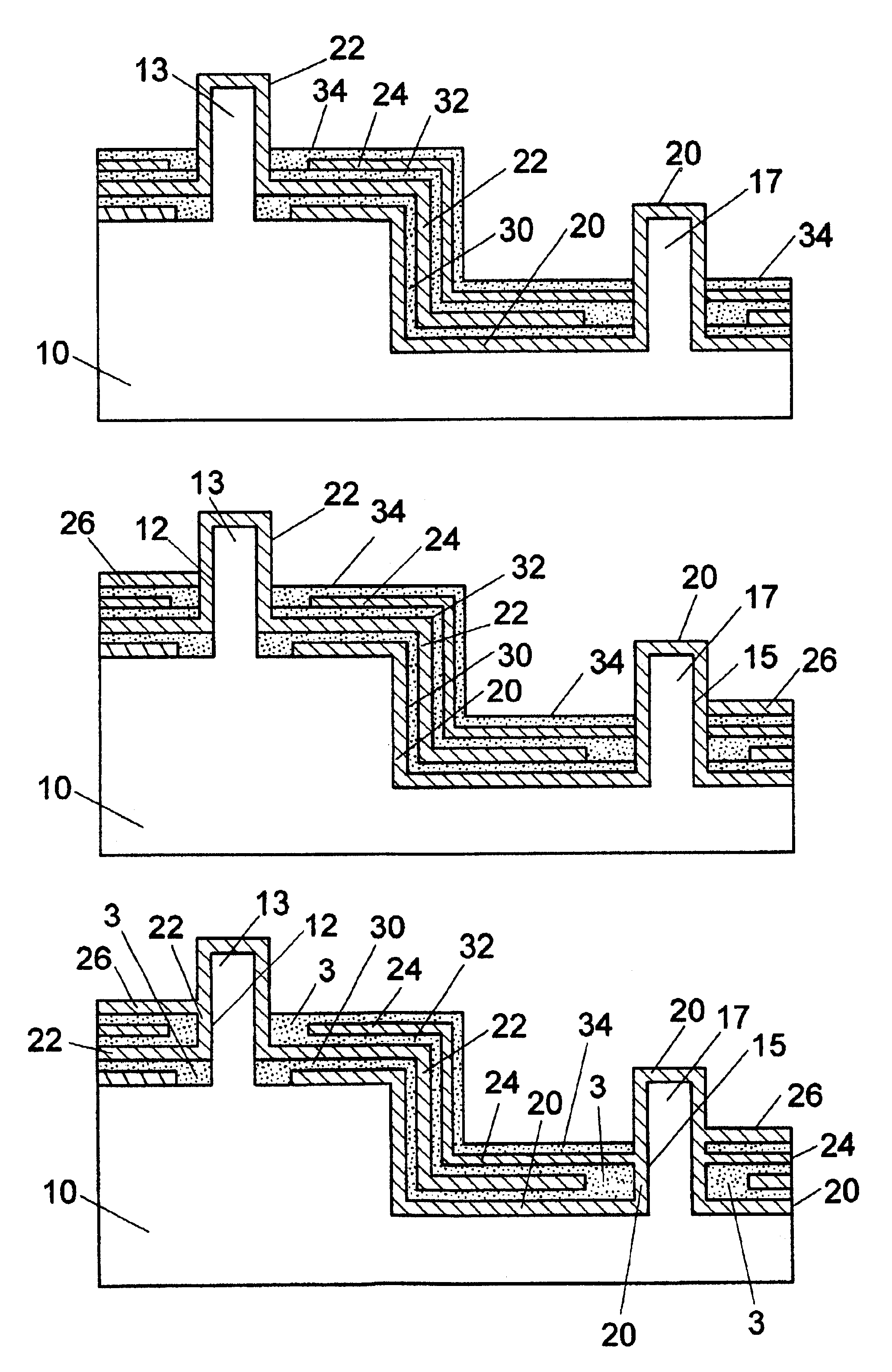
first embodiment
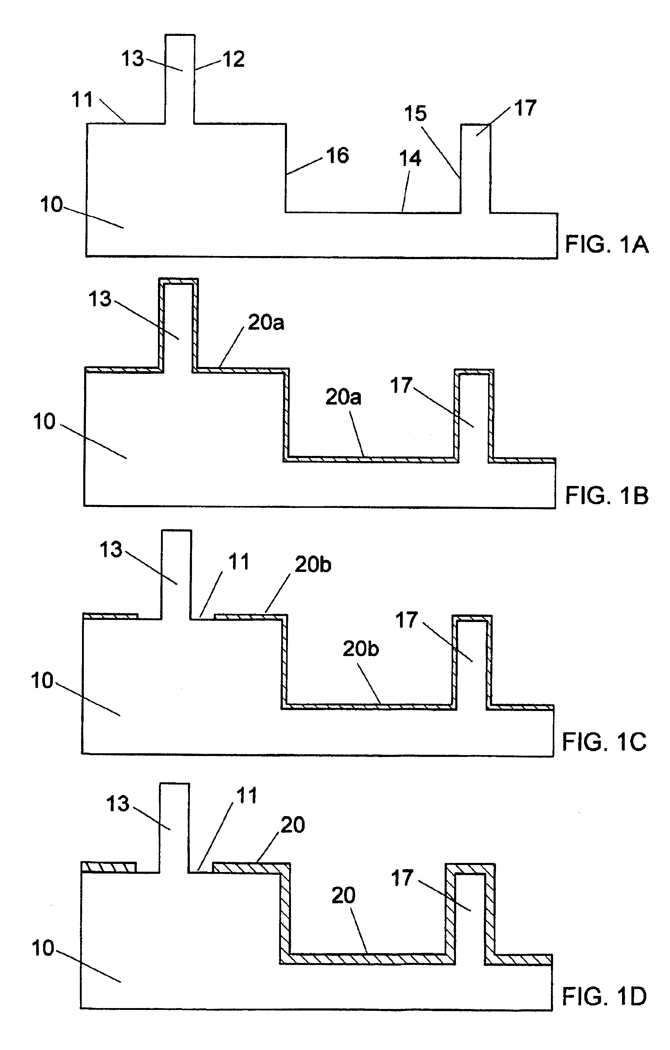
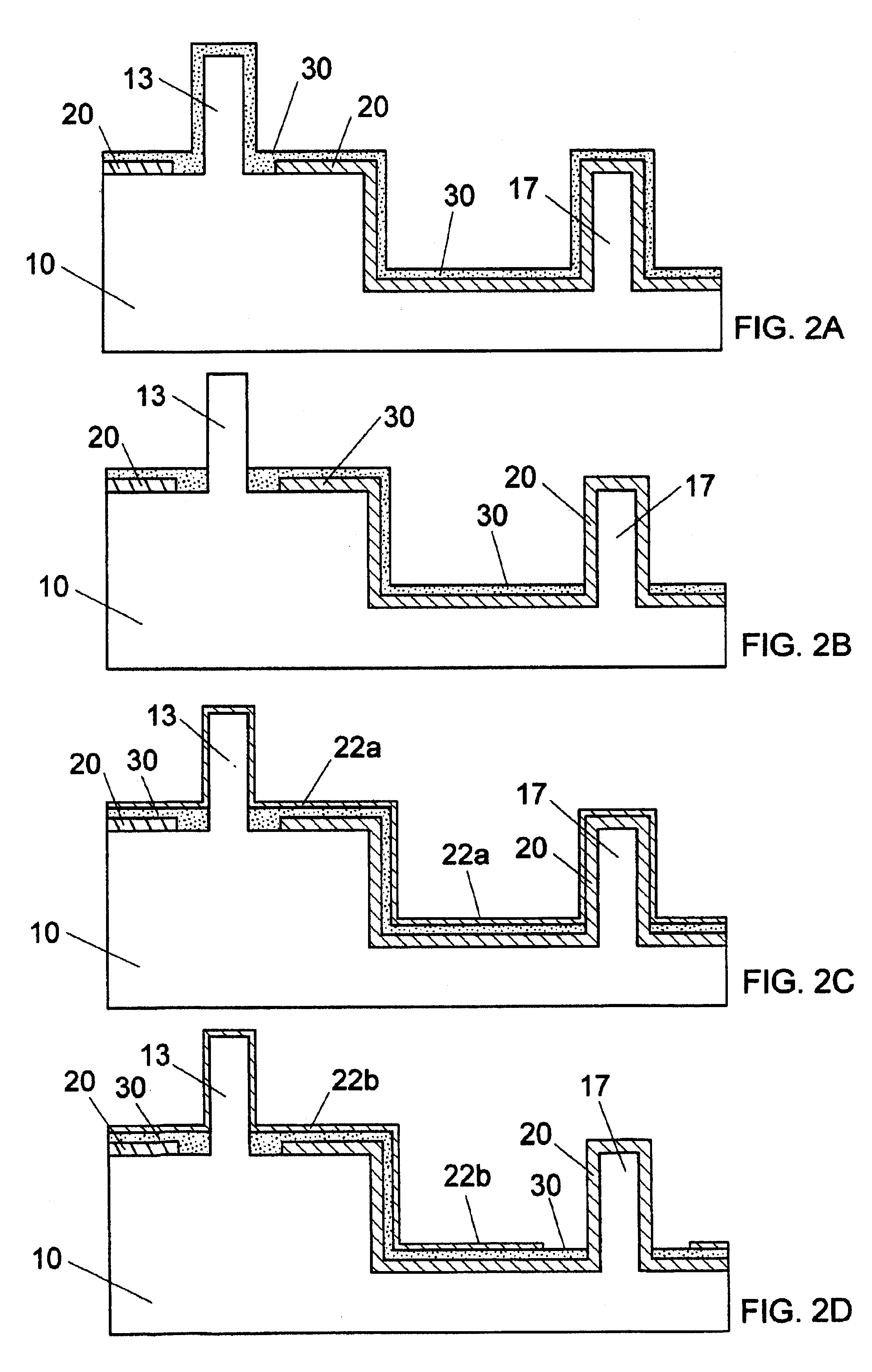
A multilayer circuit board of the first embodiment of the present invention can be manufactured by the following method.
First, a resin-molded substrate 10 for MID (molded interconnect device) is prepared. As shown in FIG. 1A, this substrate 10 has, on its top surface, a first surface 11, a first projection 13 on the first surface, second surface 14 extending at a different level from the first surface, second projection 17 on the second surface, and a third surface 16 extending between the first and second surfaces (11, 14) in a substantially vertical direction.
The substrate for MID can be three-dimensionally produced by means of injection molding. As the resin material, for example, it is possible to use polyphenylene sulfide (PPS), liquid-crystal polymer (LCP), syndiotactic polystyrene (SPS), or polyphthal amide (PPA). In addition, a filler such as inorganic fibers may be added into the resin material to improve the mechanical strength of the substrate. Alternatively, a ceramic su...
second embodiment
A multilayer circuit board according to a second embodiment of the present invention is explained in detail below.
FIG. 6 shows a cross-sectional view of the multilayer circuit board of the second embodiment. This multilayer circuit board comprises a substrate 10 having a first surface 14 that is a horizontal surface and a second surface 15 projecting in a substantially vertical direction from one side of the first surface, a multilayer circuit formed on the substrate 10 which is formed by alternately laminating a conductive layer (20, 22, 24, 26) and an insulation layer (30, 32, 34) on a required number of times. The conductive layer 20 also extends on the second surface 15, which is used to make a layer-to-layer connection between the conductive layers (20, 24).
The multilayer circuit board described above can be manufactured by the following method. First, as shown in FIG. 7A, a copper film 20a is formed on the entire first and second surfaces (14, 15) of the substrate 10 by means ...
third embodiment
A multilayer circuit board according to a third embodiment of the present invention is explained in detail below.
As shown in FIGS. 13A to 13C, this multilayer circuit board comprises a substrate 10 having a first surface 11 that is a horizontal surface, second surface 14 that is a horizontal surface extending at a different level from the first surface, and a third surface 16 extending in a substantially vertical direction between the first surface 11 and the second surface 14, and a multilayer circuit formed on the substrate 10, which is manufactured by alternately laminating a conductive layer (20, 22, 24, 26) and an insulation layer (30, 32, 34) on a required number of times. Each of the insulation layers (30, 32, 34) and the conductive layers (20, 22, 24, 26) can be formed by the same method as explained in the first embodiment. This embodiment is characterized in that a layer-to-layer connection of the multilayer circuit is made through a circuit pattern (21, 25) for layer-to-l...
PUM
| Property | Measurement | Unit |
|---|---|---|
| thickness | aaaaa | aaaaa |
| thickness | aaaaa | aaaaa |
| thickness | aaaaa | aaaaa |
Abstract
Description
Claims
Application Information