Semiconductor device manufacturing method using ultrasonic flip chip bonding technique

Inactive Publication Date: 2005-01-04
KIOXIA CORP
View PDF17 Cites 15 Cited by
  • Summary
  • Abstract
  • Description
  • Claims
  • Application Information

AI Technical Summary

Benefits of technology

FIG. 4A is a view showing the photomicrograph of the lower surface of a semiconductor chip for explaining damage to a semiconductor chip in the use of a conventional method of applying ultrasonic waves to a semiconductor chip, facing down the semiconductor chip, and mounting it on a printed circuit board;
F

Problems solved by technology

In the conventional semiconductor device manufacturing method, a bump formed on the electrode of a semiconductor chip does not uniformly contact a wiring electrode on the printed circuit board in case of insufficient parallelism adjustment between the tool and the stage or insufficient perpendicularity of the bonding surfaces of the tool and stage in the pressure direction of the tool.
This bonding state is less reliable, and the bump may come off the electrode of the semiconductor chip in the worst case.
However, these adjustments require a precision of several μm, are very difficult, and take about 2 hours regardless of any state-of-the-art apparatus.
However, a semiconductor chip as thin as 100 μm or less is damaged by ultrasonic vibrations in flip chip connection, generating a defect such as a scratch or crack.
When a sealing resin layer is interposed between a semiconductor chip and a printed circuit board and simultaneous flip chip connection including the sealing step is performed, the semiconductor chip deforms due to the resin stress concentrated in the chuck hole because of a thin semiconductor chip, damaging the semiconductor chip.
For this reason, a load enough for bonding cannot be applied between the semiconductor chip and the printed circuit board.
However, the former method increases the number of manufacturing steps, whereas the latter method decreases the tool durability by ultrasonic vibrations.
Either method is not a permanent measure.
As described above, it is difficult for the conventional semiconductor device manufacturing method to improve the connectivity.
A thin semiconductor chip may be damaged in flip chip connection.

Method used


Image

  • Semiconductor device manufacturing method using ultrasonic flip chip bonding technique
  • Semiconductor device manufacturing method using ultrasonic flip chip bonding technique
  • Semiconductor device manufacturing method using ultrasonic flip chip bonding technique

Examples


first embodiment

[First Embodiment]

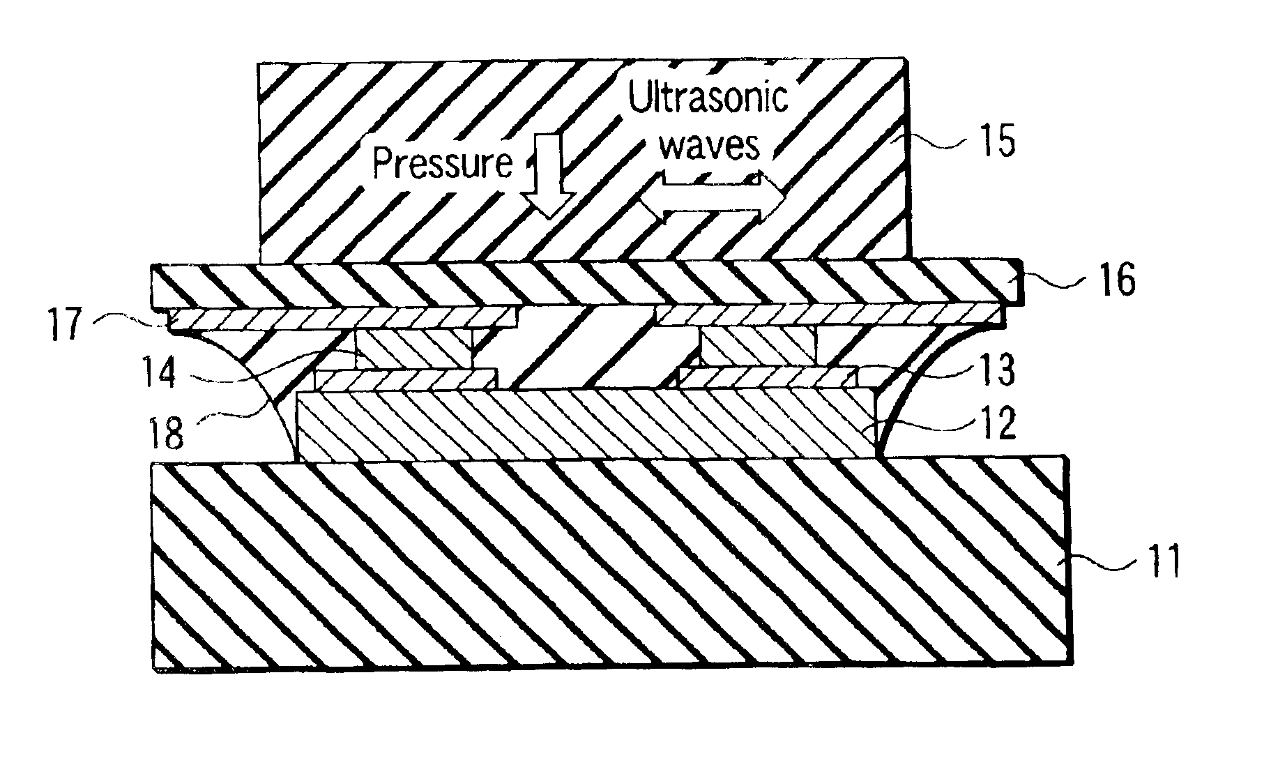
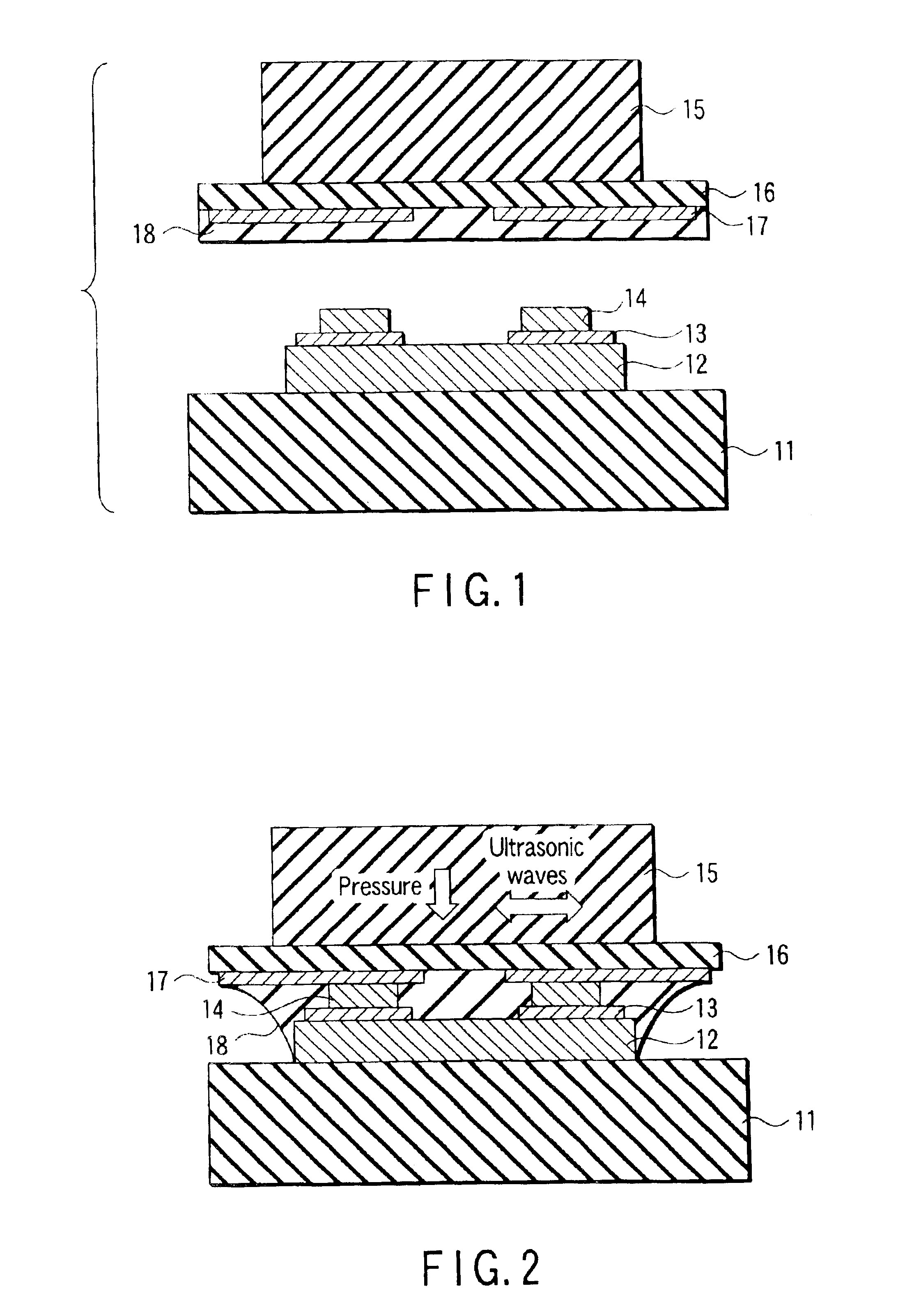
FIG. 6 is a flow chart showing a manufacturing process regarding the ultrasonic flip chip bonding technique for explaining a semiconductor device manufacturing method according to the first embodiment of the present invention. Various elements are formed in a semiconductor substrate (wafer) by a known process. The wafer is then diced into chips along the dicing line or scribe line of the wafer by using a diamond scriber, diamond blade, laser scriber, or the like, thereby forming a semiconductor chip 12.

A stud bump 14 is formed on an electrode 13 of the chip 12 (STEP 1). The element formation surface (upper chip surface) of the chip 12 is coated with a sealing material 18 by spin-coating, e.g., a liquid resin (STEP 2). The sealing material 18 can also be formed by adhering a resin sheet. The lower surface of the chip 12 is chucked and fixed onto a porous stage 11 (STEP 3).

A printed circuit board 16 for mounting the chip 12 is picked up (STEP 4). A surface of the pri...

second embodiment

[Second Embodiment]

FIG. 7 is a flow chart showing a manufacturing process regarding the ultrasonic flip chip bonding technique for explaining a semiconductor device manufacturing method according to the second embodiment of the present invention. Various elements are formed in a semiconductor substrate (wafer) by a known process. The wafer is then diced into chips along the dicing line or scribe line of the wafer by using a diamond scriber, diamond blade, laser scriber, or the like, thereby forming a semiconductor chip 12.

The element formation surface (upper chip surface) of the chip 12 is coated with a sealing material 18 by spin-coating, e.g., a liquid resin (STEP 1). The sealing material 18 can also be formed by adhering a resin sheet. The chip 12 is chucked and fixed onto a porous stage 11 (STEP 2). A stud bump is formed on a wiring electrode 17 of a printed circuit board 16 (STEP 3).

The printed circuit board 16 for mounting the chip 12 is picked up (STEP 4). A surface of the pr...

third embodiment

[Third Embodiment]

FIG. 8 is a flow chart showing a manufacturing process regarding the ultrasonic flip chip bonding technique for explaining a semiconductor device manufacturing method according to the third embodiment of the present invention. Various elements are formed in a semiconductor substrate (wafer) by a known process. The wafer is then diced into chips along the dicing line or scribe line of the wafer by using a diamond scriber, diamond blade, laser scriber, or the like, thereby forming a semiconductor chip 12.

A stud bump 14 is formed on an electrode 13 of the chip 12 (STEP 1). The element formation surface (upper chip surface) of the chip 12 is coated with a sealing material 18 by spin-coating, e.g., a liquid resin (STEP 2). The sealing material 18 can also be formed by adhering a resin sheet. The lower surface of the chip 12 is chucked and fixed onto a porous stage 11 (STEP 3).

A stud bump is formed on a wiring electrode 17 of a printed circuit board 16 (STEP 4).

The print...


PUM


Abstract

A bump is formed on at least one of a semiconductor chip and printed circuit board. A sealing material is applied to the surface of one of the semiconductor chip and printed circuit board. The printed circuit board is flip-chip-connected to the semiconductor chip via the sealing material while ultrasonic waves are applied to the printed circuit board to promote bonding by the bump.

Description

CROSS-REFERENCE TO RELATED APPLICATIONSThis application is based upon and claims the benefit of priority from the prior Japanese Patent Application No. 2002-060700, filed Mar. 6, 2002, the entire contents of which are incorporated herein by reference.BACKGROUND OF THE INVENTION1. Field of the InventionThe present invention relates to a semiconductor device manufacturing method and, more particularly, to an ultrasonic flip chip bonding technique of packaging a flip chip.2. Description of the Related ArtIn an ultrasonic flip chip bonding technique, a printed circuit board is chucked by a heatable fixing jig called a stage. A semiconductor chip (semiconductor element) is packaged while being chucked by an apparatus having a pressure & ultrasonic application mechanism called a tool or a mechanism also using heating. At this time, the element formation surface of the semiconductor chip and the wiring electrode formation surface of the printed circuit board are faced to each other in orde...

Claims


Application Information

Patent Timeline
IPC IPC(8): H01L21/60H01L23/48H01L23/498H01L21/02
CPCH01L23/4985H01L24/81H01L2224/73204H01L2224/32225H01L2224/16225H01L2924/01074H01L2924/01033H01L2224/83192H01L2224/83191H01L2224/81801H01L2224/81208H01L2224/81205H01L2224/16H01L2924/00H01L2224/05568H01L2224/05573H01L2924/00014H01L2924/12042H01L2224/05599
Inventor IIZUKA, KAZUHIROTAKYU, SHINYA
Owner KIOXIA CORP
Why Eureka
Try Eureka