Active matrix substrate

a technology of active matrix and substrate, which is applied in the direction of discharge tube luminescnet screen, instrumentation, and semiconductor/solid-state device details, etc., can solve the problems of static electricity having the potential to destroy thin film devices comprising thin dielectric layers, susceptibility to damage, etc., to discourage current flow, dissipate negative charge build-up, and discourage current flow

Inactive Publication Date: 2005-01-04
TPO HONG KONG HLDG
View PDF15 Cites 6 Cited by
  • Summary
  • Abstract
  • Description
  • Claims
  • Application Information

AI Technical Summary

Benefits of technology

This may be achieved by doping a semiconductor region of the ESD protective circuitry so as to provide a gentle conductive path from the part of that semiconductor region connected to a row conductor through that semiconductor region to the external environment of the substrate, and to discourage current flow through that semiconductor region in the opposite direction.
Alternatively, for dissipating negative charge build-up on the substrate, a semiconductor region of the ESD protective circuitry may be doped so as to provide a gentle conductive path from external environment of the substrate, through that semiconductor region and to the part of that semiconductor region connected to a row conductor, and to discourage current flow through that semiconductor region in the opposite direction.

Problems solved by technology

As is well known, static electricity has the potential to destroy thin film devices comprising thin dielectric layers and of particular susceptibility to damage are the gate regions of MOS TFTs.

Method used


Image

  • Active matrix substrate
  • Active matrix substrate
  • Active matrix substrate

Examples


Embodiment Construction

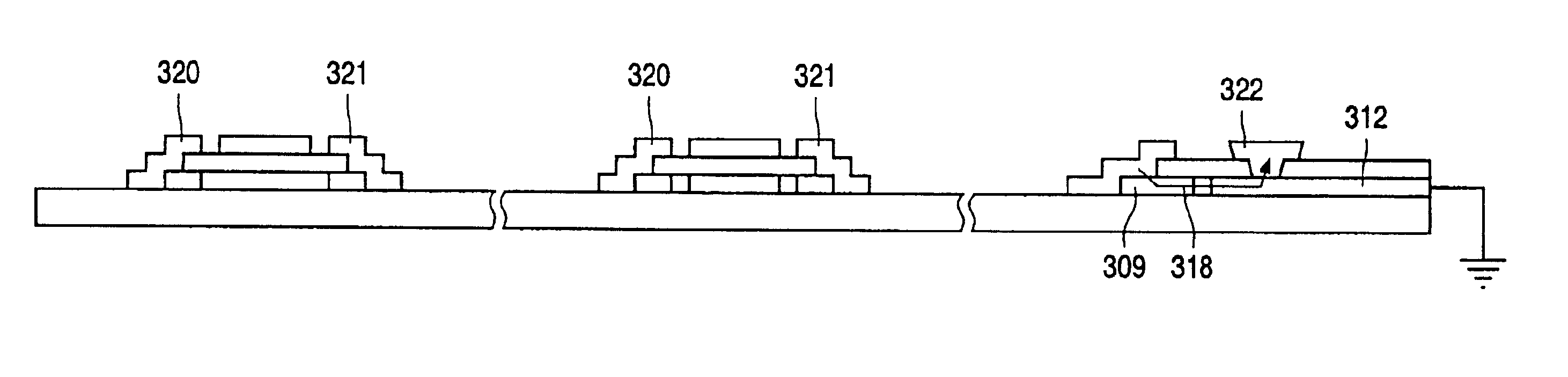
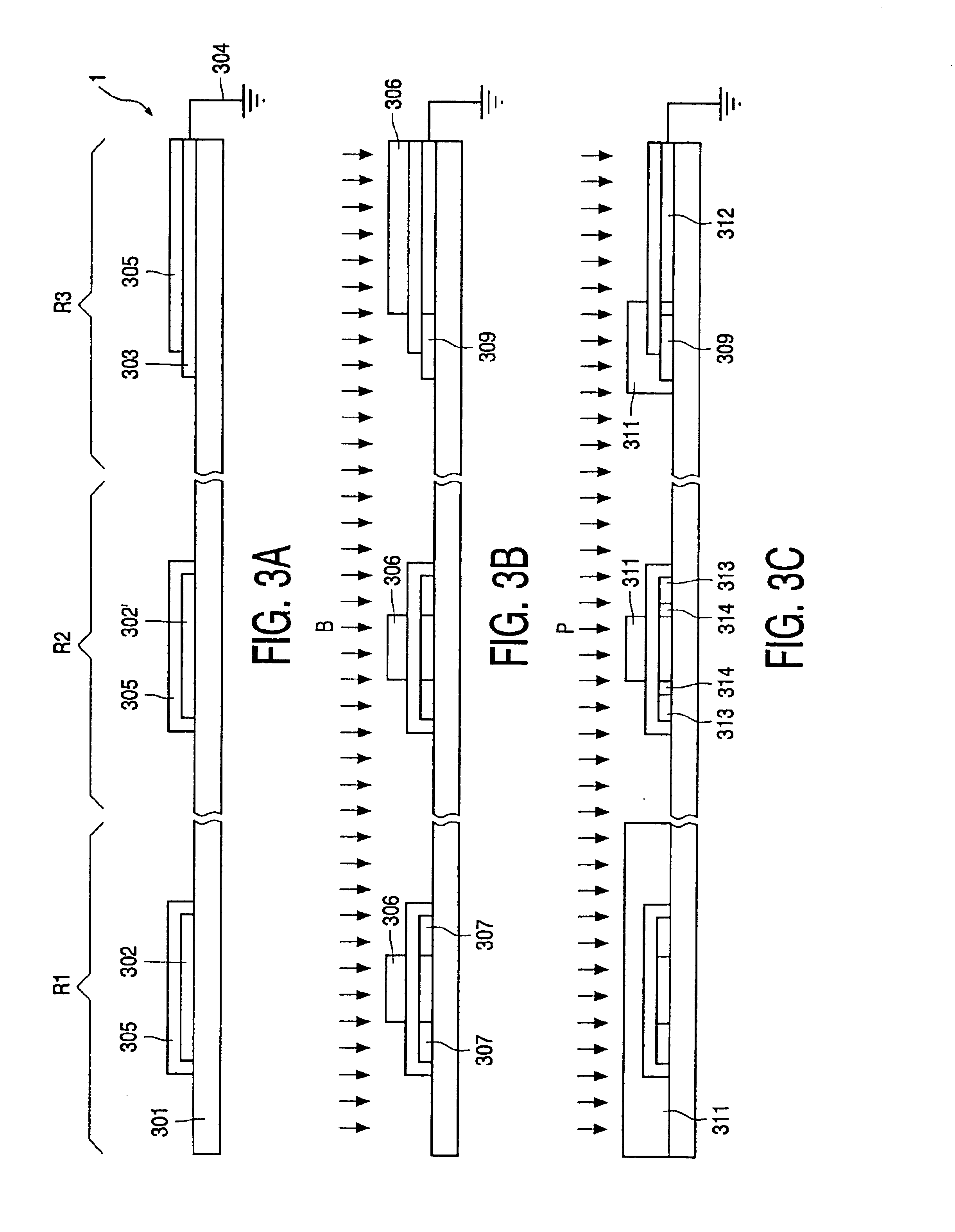
It should be noted that the drawings are schematic and relative dimensions and proportions of parts of the cross-section views and circuit layout have been exaggerated or reduced in size for the sake of clarity. The same reference signs are generally used to refer to corresponding or similar features in different embodiments.

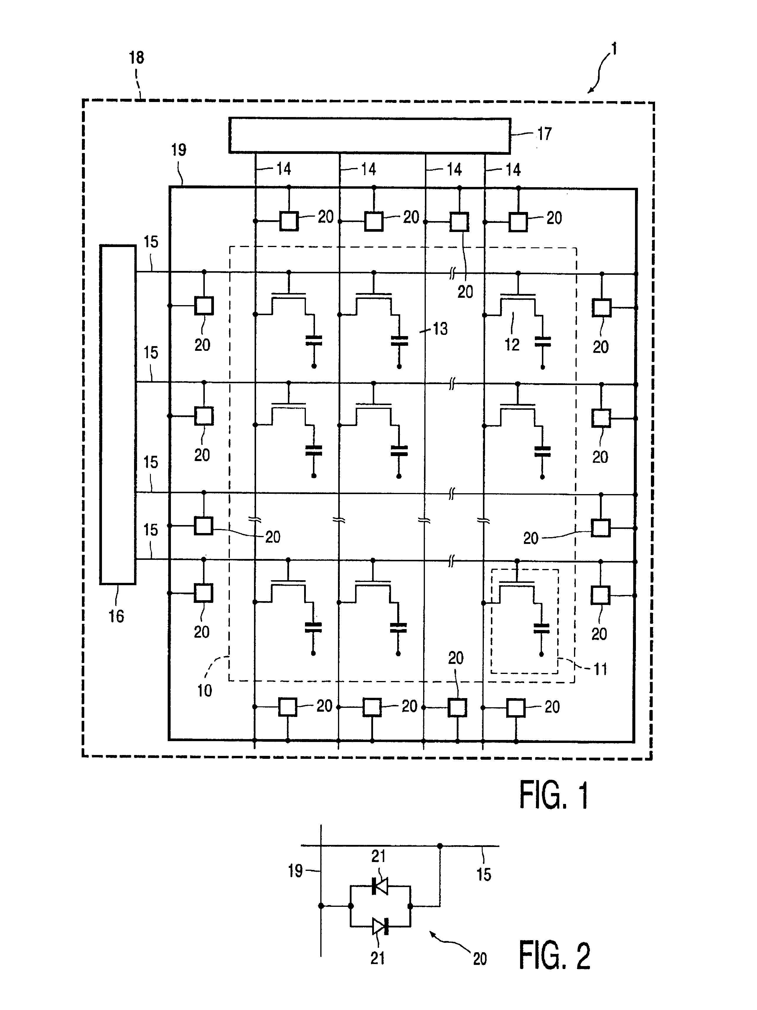
In FIG. 1, an AMLCD 1 manufactured by a method according to the present invention is shown comprises an display area 10 on a display panel 18, the display area consisting of m rows (1 to m) and n columns (1 to n) of identical picture elements 11. Only a few of the picture elements are shown for simplicity whereas in practice, the total number of picture elements (m×n) in the display area 10 may be 200,000 or more. Each picture element 11 has a picture electrode 12 and associated therewith a switching TFT 13 of the type manufactured by the method illustrated in FIGS. 1A to 1D, and which serves to control the application of data signal voltages to the picture elec...


PUM

PropertyMeasurementUnit
sizeaaaaaaaaaa
semiconductoraaaaaaaaaa
conductiveaaaaaaaaaa

Abstract

An active matrix substrate includes a row and column array of active elements. Each element is associated with a TFT having a gate electrode connected to a corresponding row conductor and source and drain (electrodes connected to corresponding column conductors. Circuitry for protecting against electrostatic discharge (ESD) is connected to at least one of the row conductors for protecting the TFTs against ESD.

Description

FIELD OF TECHNOLOGYThis invention relates to a method of manufacturing an active matrix substrate comprising a row and column array of active elements, each element being associated with a switching thin film transistor (TFT), and ESD protective circuitry connected to the TFTs for protecting against electrostatic discharge (ESD). In particular, but not exclusively, the invention relates to the manufacture of active matrix substrates using complementary metal oxide semiconductor (CMOS) technology, for example, an active matrix liquid crystal display (AMLCD) having CMOS based TFTs switching TFTs or CMOS based integrated row and column driver circuitry.BACKGROUND AND SUMMARYThe invention is described hereafter with reference to AMLCDs, however, it will be appreciated that the invention is not merely limited to AMLCDs but has application with respect to other types of large area electronic devices such as thin film data stores or image sensors.As is well known, static electricity has th...

Claims


Application Information

Patent Timeline
Patent Type & Authority Patents(United States)
IPC IPC(8): H01L27/02H01L27/04G02F1/1362H01L21/822H01L21/8238H01L27/06H01L27/08H01L27/092H01L27/12H01L29/786
CPCG02F1/136204H01L27/0255H01L27/12G02F1/136
Inventor TRAINOR, MICHAEL J.AYRES, JOHN R. A.
Owner TPO HONG KONG HLDG
Why Eureka
Try Eureka