Package and method for making an underfilled integrated circuit

a technology for integrated circuits and packaging, applied in the field of packaging and method for making an integrated circuit, can solve the problems of poor application effect of underfill material, low production efficiency, and inability to meet the requirements of the package assembly, etc., and achieve the effect of efficient and complete application of underfill material

Inactive Publication Date: 2005-01-04
ADVANCED MICRO DEVICES INC
View PDF22 Cites 12 Cited by
  • Summary
  • Abstract
  • Description
  • Claims
  • Application Information

AI Technical Summary

Benefits of technology

The present invention provides a novel package board, for use in flip-chip integrated circuit manufacturing, that has a depression having package connector pads. An integrated circuit die, having solder bumps thereon, is positioned in the depression by a die placement tool. The walls of the depression align the die with the package connector pads and hold the die in place. The package and die, which together form an integrated circuit package assembly, are moved together from the die placement tool into a reflow furnace. The depression holds the die in place during the reflow step, thereby ensuring that the die will remain aligned with the connector pads on the package board surface. Thus, the present invention satisfies the need for a package board that aligns the die with the package connector pads while holding the die in place before and during the reflowing step.
The present invention also provides for a package board having a depression, wherein at least one of the walls of the depression has an indentation. The indentation is adapted to receive underfill material. The indentation may extend from one wall to another, or it may extend across only a portion of a wall. The indentation permits underfill material, such as a polymerizable material, to be introduced to the underside of the die after the reflow step has been completed. The indentation in the depression allows for application of the underfill material in fewer steps (as few as a single step) than is possible with prior art package boards having no depression. The depression acts as a reservoir for the underfill material, allowing the underfill material to completely and evenly fill the gaps between the die, package board and solder connections. Thus, the package board of the present invention also satisfies the need in the art for a package board that permits more efficient and complete application of underfill material.
The unique package board according to the present invention, when combined with a die, forms an integrated circuit package assembly wherein the die is held in place by the depression as it passes from a die placement tool to a reflowing oven. The reflowed integrated circuit package is then permitted to cool, after which underfill material is dispensed into the indentation, whence it flows into the depression, completely filling the gaps beneath the underside of the die. The underfill material may be applied in a single step, resulting in a single, cohesive layer of adhesive, which joins the die to the package surface. Because the underfill need not be layered, as is required in prior art processes, when the underfill material hardens, it holds the die in place with greater adhesive strength than would be possible using flat package boards according to prior art methods. Thus, the present invention also provides for an underfilled integrated circuit package that is superior in strength and durability when compared to prior art packages. Thus, the present invention satisfies the need in the art for an integrated circuit die and package assembly having superior strength and durability.

Problems solved by technology

Interconnection and packaging related issues are among the main factors that determine not only the number of circuits that can be integrated on a chip, but also the performance of the chip.
Prior art methods of manufacturing an underfilled integrated circuit package assembly have disadvantages, however.
One disadvantage to prior art processes is that a flat package board permits the die to move around thereon.
Thus the die will often move and become misaligned after the die is positioned on the package board, but prior to reflowing of the solder balls.
This results in defective products, with concomitant economic loss.
Another disadvantage of prior art methods of manufacturing an integrated circuit is that prior art methods require that underfill material be applied in multiple iterations of small increments.
This leads to increased process time, which increases economic costs.
Additionally, prior art processes apply underfill material in layers, which results in a weaker adhesive effect than would be obtainable using a single layer of underfill material, since multiple layers have a tendency to separate or delaminate along the interstices of the layers.
Also, prior art processes result in uneven application of underfill material, which often results in pockets of air remaining within the underfill material.
These pockets of air can cause premature corrosion of solder connectors, uneven heat dissipation from the die, and other undesirable phenomena.

Method used


Image

  • Package and method for making an underfilled integrated circuit
  • Package and method for making an underfilled integrated circuit
  • Package and method for making an underfilled integrated circuit

Examples


Embodiment Construction

The present invention provides overcomes the deficiencies in the prior art by providing a unique package board having a depression that receives and holds in place an integrated circuit die, wherein at least one wall of the depression has an for receiving underfill material.

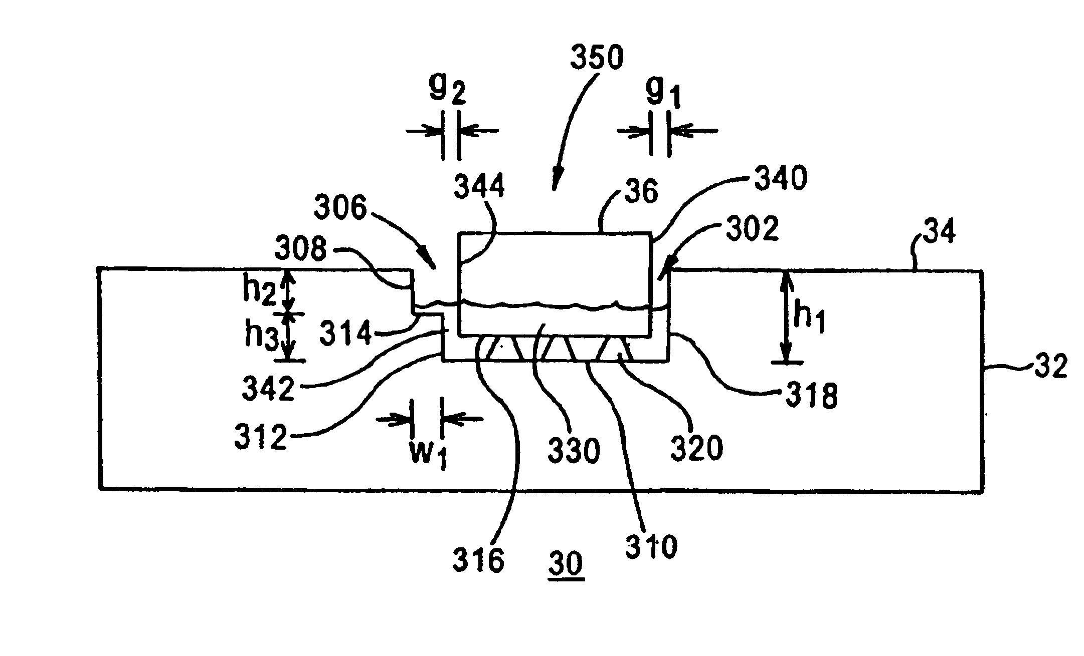
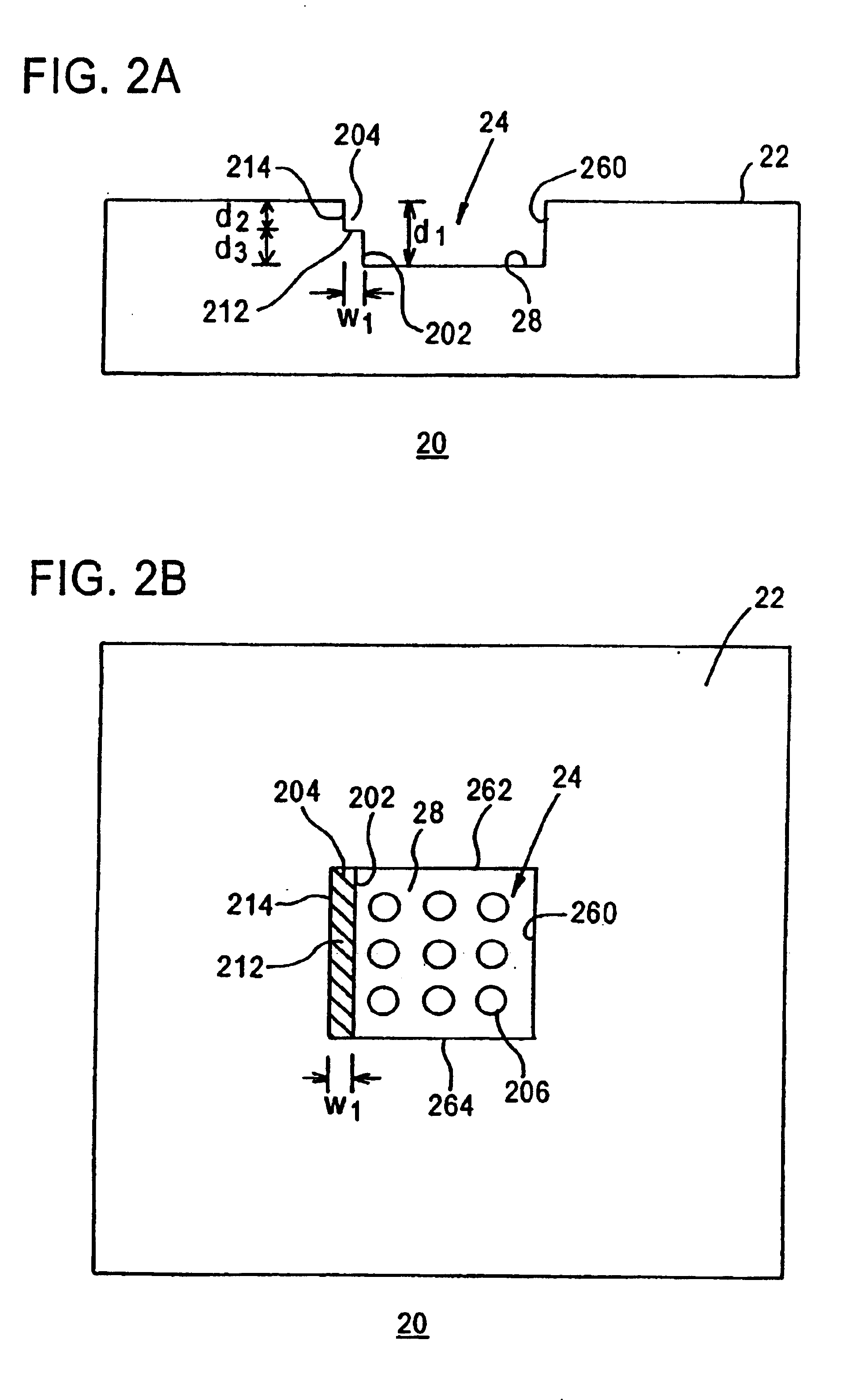
FIGS. 2A and 2B depict a side cross-sectional view and a top view, respectively, of an exemplary package board 20 according to the present invention. The package board 20 has a top surface 22 and contains a depression 24. The depression 24 has a floor 28, three substantially vertical walls 260, 262, 264 and indented wall 202. Indented wall 202 contains indentation 204. The indentation 204 has a base 212 and a bulkhead 214. The base 212 of indentation 204 lies at an indentation base height d3 above the floor 28 of the depression 24. The base 212 of indentation 204 lies at an indentation base depth d2 lower than the top surface 22. The floor 28 lies at a depression floor depth d1 lower than the top surface 22. Thus...


PUM


Abstract

An integrated circuit package for use in flip-chip manufacturing has a surface having a depression for receiving a bumped die. The depression has disposed on its floor a plurality of cage pads. The depression has four walls, at least one of which is indented to form a step. In the flip-chip manufacturing process, a bumped die is positioned within the depression so that the solder bumps line up with the cage pads, and is precisely aligned and held in place by the depression. The die-package combination is then heated in a furnace to reflow the solder bumps, thus forming an integrated circuit. Using the indentation in the depression, underfill material is introduced into the depression. The underfill material flows into the depression and under the die, surrounding the reflowed solder bumps.

Description

BACKGROUND OF THE INVENTION1. Field of the InventionThe present invention relates to the packaging of integrated circuits and electronic components, and more particularly, to an improved package for use in flip-chip manufacturing of an underfilled integrated circuit package.2. Description of the Related ArtInterconnection and packaging related issues are among the main factors that determine not only the number of circuits that can be integrated on a chip, but also the performance of the chip. These issues have increased in importance as advances in chip design have led to reductions in the sizes of features on transistors and enlargements in chip dimensions. Industry has come to realize that merely having a fast chip will not result in a fast system; it must also be supported by equally fast and reliable packaging.Essentially, packaging supplies the chip with signals and power, and performs other functions such as heat removal, physical support and protection from the environment. ...

Claims


Application Information

Patent Timeline
Patent Type & Authority Patents(United States)
IPC IPC(8): H01L21/56H01L23/13H01L23/12H01L21/02
CPCH01L21/563H01L24/32H01L23/13H01L2924/01076H01L2224/16225H01L2224/27013H01L2224/73203H01L2224/83051H01L2924/01005H01L2924/14H01L2924/15153H01L2924/15157H01L2924/15165H01L2224/32225H01L2224/73204H01L2924/01033H01L2924/01006H01L2924/00
Inventor MONTIEL, FRANK
Owner ADVANCED MICRO DEVICES INC
Why Eureka
Try Eureka