Display driving device and manufacturing method thereof and liquid crystal module employing the same

a technology of display element and driving device, which is applied in static indicating devices, instruments, non-linear optics, etc., can solve the problems of increasing load capacity of clock signal lines, reducing load capacity, and aggravate the waveform rounding and delay of clock signals. the effect of accurate driving of liquid crystal panels

Inactive Publication Date: 2005-01-04
SHARP KK
View PDF9 Cites 33 Cited by
  • Summary
  • Abstract
  • Description
  • Claims
  • Application Information

AI Technical Summary

Benefits of technology

Thus, when the start pulse signal is transferred to the driving semiconductor element on the following stage, the synchronize clock signal to be used for outputting a signal to be a source of the drive signal precedes the clock signal used in the driving semiconductor element of the preceding stage with respect to the start pulse signal by the phase difference which corresponds to the sum of transfer time of the input buffer of a single stage and the output buffer of a single stage and which corresponds to the delay time due to waveform rounding. As a result, the start pulse signal for-generating the drive signal is inputted at a correct timing and the liquid crystal module operates correctly.
Thus, the same manufacturing steps can be used for all tape carrier packages up until the film cutting step, and the tape carrier package of the last stage and the other tape carrier packages can be separated from each other at the film cutting step, thereby efficiently manufacturing the above display driving device. Also, even when the arrangement of the input / output terminals of the driving semiconductor elements are altered, the tape carrier package can be manufactured only by changing the shorted portion, thus improving the degree of freedom of the serial connection.
In accordance with the invention, the display driving device is provided as a group of gate drivers or a group of source drivers for driving pixels on the liquid crystal panel, thus accurately driving the liquid crystal panel.

Problems solved by technology

As a result, in the subsequent operation, the start pulse signal SPG is transferred while maintaining this incorrectness and there occurs malfunction of the liquid crystal module 501.
As a result, increase in load capacity of the clock signal line further aggravates the waveform rounding and delay of the clock signal.
Further, because the data signal and clock signal need to be made faster to keep up with the increased number of pixels, the timing control of these signals are becoming harder than ever.
For these reasons, in timing control, there is a limit in conventional techniques in which the load capacity is reduced by micro technique, and in which the driving capacity of the input / output buffer circuit of the clock signal is enhanced to meet the demand of various conditions such as above required for the liquid crystal module, and such conventional techniques involve difficulty in design of mounting as a liquid crystal module.

Method used


Image

  • Display driving device and manufacturing method thereof and liquid crystal module employing the same
  • Display driving device and manufacturing method thereof and liquid crystal module employing the same
  • Display driving device and manufacturing method thereof and liquid crystal module employing the same

Examples


first embodiment

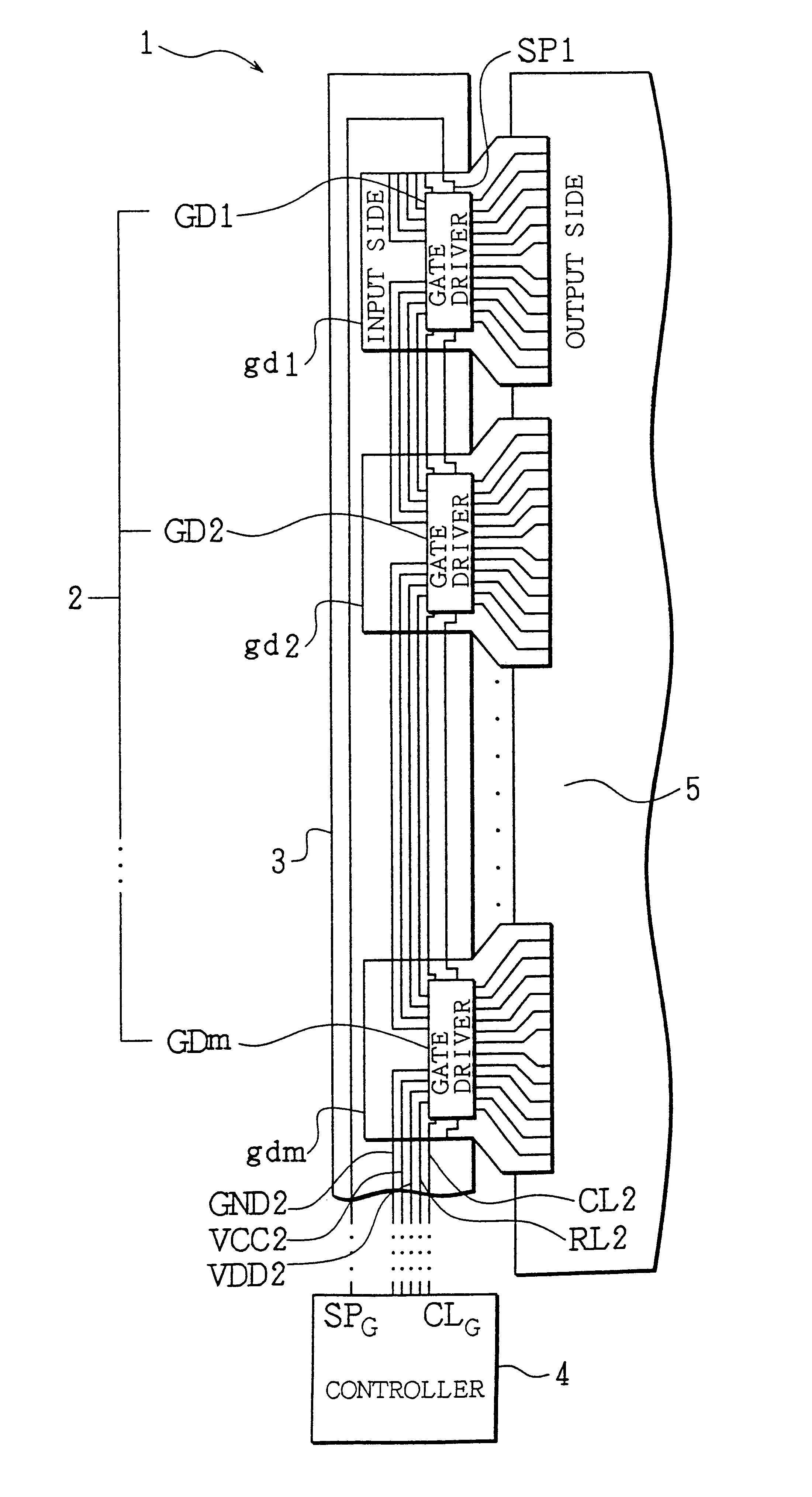
The following will describe one embodiment of a display driving device of the present invention and a liquid crystal module employing such a display driving device referring to FIG. 1 through FIG. 8. Note that, even though the following explanations are based on a group of gate drivers as an example of the display driving device, the features of such a group of gate drivers and the liquid crystal module employing it are obviously applicable to a group of source drivers as well.

FIG. 1 shows a structure of a liquid crystal module 1 of the present embodiment. The liquid crystal module 1 includes a group of gate drivers 2, a print substrate 3 bearing wiring for the group of gate drivers 2, a controller 4 for supplying a signal required for driving liquid crystal to the group of gate drivers 2, and a liquid crystal panel 5 which is driven by the group of gate drivers 2.

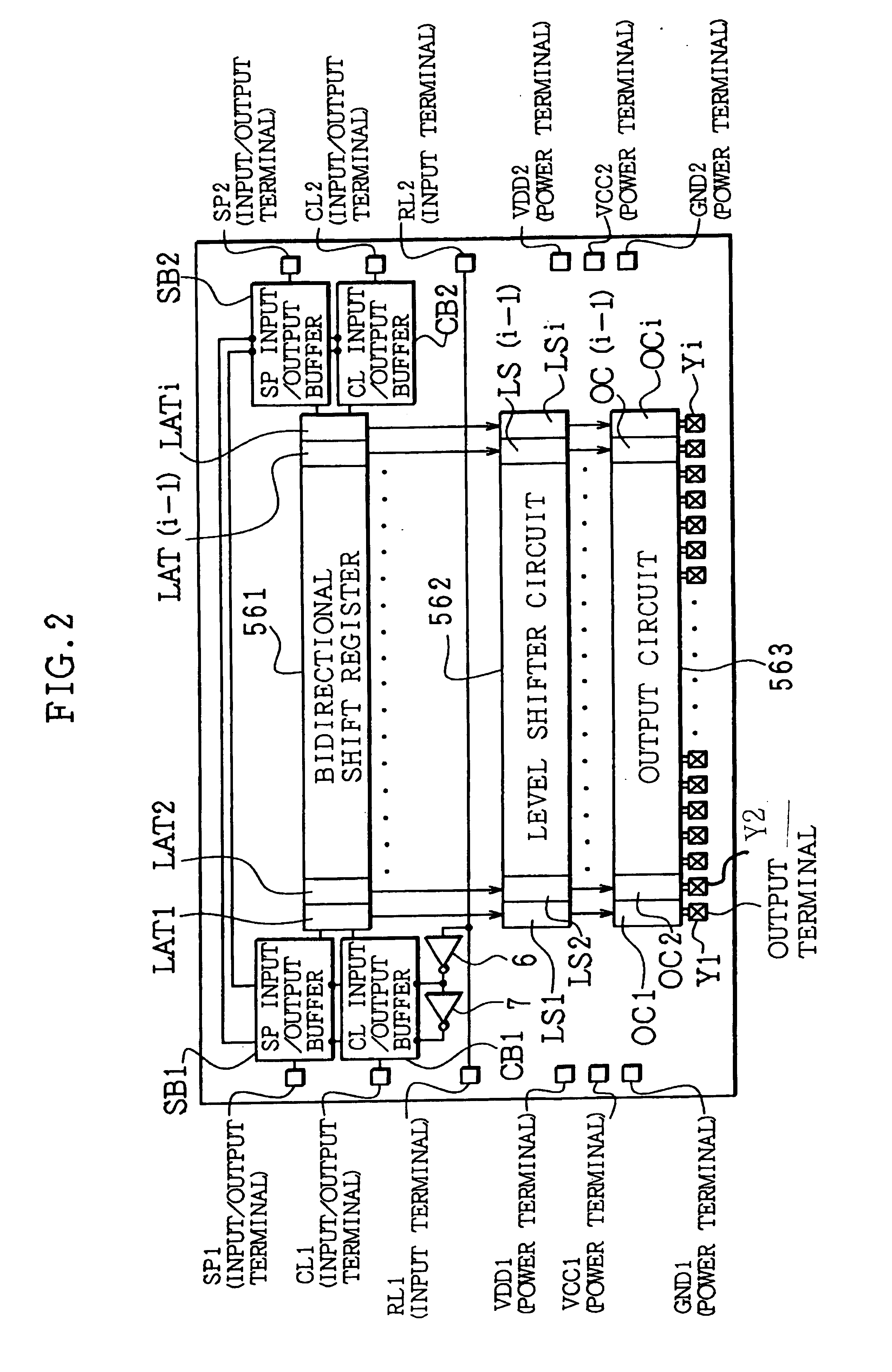
The group of gate drivers (display driving device) 2 is composed of m gate drivers (driving semiconductor elements) GD1,...

second embodiment

The following will describe another embodiment of the display driving device of the present invention and the liquid crystal module employing it referring to FIG. 9 through FIG. 17. Note that, for convenience of explanation, those constituting elements having the same functions as those described in FIG. 1 are given the same reference numerals and explanations thereof are omitted here. Also, even though the following explanation is based on a group of gate drivers as an example of the display driving device, as with the First Embodiment, the features of such a group of gate drivers and the liquid crystal module employing it are obviously applicable to a group of source drivers as well.

FIG. 9 and FIG. 10 show the structures of liquid crystal modules 111 and 112 of the present embodiment, respectively. Unlike the First Embodiment in which the wiring from the controller 4 to the input / output terminal SP1 or SP2 of the gate driver to which the start pulse signal SPG is first inputted is...


PUM

PropertyMeasurementUnit
forward voltageaaaaaaaaaa
voltageaaaaaaaaaa
gate voltageaaaaaaaaaa

Abstract

A gate driver mounted on a TCP is mounted on a print substrate. The input / output terminal, input terminal, and power terminal of the gate driver at one end of a group of gate drivers are connected to a controller by this mount, and a clock signal, select signal, and power voltage are transferred in a direction of the gate drivers. Meanwhile, the input terminal of a gate driver at the other end of the group of gate drivers is connected to the controller, and a start pulse signal is transferred in a direction of the gate drivers. As a result, it is possible to provide a display driving device in which a start pulse signal is fed in at a correct timing, a manufacturing method thereof, and a liquid crystal module employing such a display driving device.

Description

FIELD OF THE INVENTIONThe present invention relates to a driving device for driving a display element for image display, and in particular to a connection mode and signal supplied mode of liquid crystal drivers installed as gate drivers and source drivers in a liquid crystal module.BACKGROUND OF THE INVENTIONThe following will describe a conventional TFT-LCD module (liquid crystal module) referring to FIG. 18. A TFT-LCD module 501 of FIG. 18 is composed of a group of gate drivers (gate electrode drive circuit) 530, a group of source drivers (source electrode drive circuit) 540, a liquid crystal panel 550, a controller 510, and a liquid crystal power circuit 520.The group of gate drivers 530 is composed of m gate drivers G1, G2, . . . , and Gm, which are LSI (Large Scale Integrated Circuit) chips of multiple outputs for driving gate bus lines of the liquid crystal panel 550. Each gate driver is mounded on a TCP (Tape Carrier Package) composed of copper foil wiring which is patterned ...

Claims


Application Information

Patent Timeline
Patent Type & Authority Patents(United States)
IPC IPC(8): G02F1/133G02F1/13G02F1/1345G09G3/36G09G3/20
CPCG09G3/3677G09G3/3688G09G2310/0289G09G2300/0426G02F1/133
Inventor ORISAKA, YUKIHISAOGAWA, YOSHINORI
Owner SHARP KK
Why Eureka
Try Eureka