Apparatus and method for cleaning test probes

a technology for cleaning apparatus and test probes, applied in the field of probe cards, can solve the problems of dies being “bad” (non-functional), pad material to the probe tip may contaminate the probe elements, and the dies being “good” (full function)

Inactive Publication Date: 2005-01-11
FORMFACTOR INC
View PDF23 Cites 27 Cited by
  • Summary
  • Abstract
  • Description
  • Claims
  • Application Information

AI Technical Summary

Problems solved by technology

In practice, however, certain physical defects in the wafer itself and certain defects in the processing of the wafer inevitably lead to some of the dies being “good” (fully-functional) and some of the dies being “bad” (non-functional).
Upon contact and penetration of the pad material by the probe tips, the transfer of the pad material to the probe tips may contaminate the probe elements.
Even non-wiping contacts may become contaminated during probing, both by material transfer and / or alloying, as well as by adhering of loose particles of debris to the side of the probe element.
Foreign debris is not limited to only metal shavings and / or metal oxide chips, however, but may also include matter such as dust, polymeric or metallic oxide by-products resulting from the various process performed on wafers associated with the building of integrated circuits, or any other material that may interfere with obtaining a proper electrical connection between the probe tip and the die surface, or proper positioning of the probe itself in relation to the die.
A disadvantage of the above described conventional cleaning process is that the portions of base material (e.g., silicone rubber) and / or abrasive particles (e.g., abrasive grains) may fall or chip off the abrading pad during the pressing-and-extracting process, thereby producing additional foreign material that may stick to the probe tips.
The use of such solvents is undesirable for many reasons.
For example, the blowing of an organic solvent is time consuming and may be messy or hazardous.
Additionally, blowing of dry air is time consuming.
A disadvantage of this cleaning process is that an operator must typically swap the abrading pad with the gel pad during the cleaning process, because testing systems typically include only one auxiliary tray for holding such pads.
This is undesirable because it prevents wafer testing from being a completely automated process, thereby significantly reducing wafer testing throughput.

Method used


Image

  • Apparatus and method for cleaning test probes
  • Apparatus and method for cleaning test probes
  • Apparatus and method for cleaning test probes

Examples


Embodiment Construction

Table of Contents

I. Terminology of the Invention

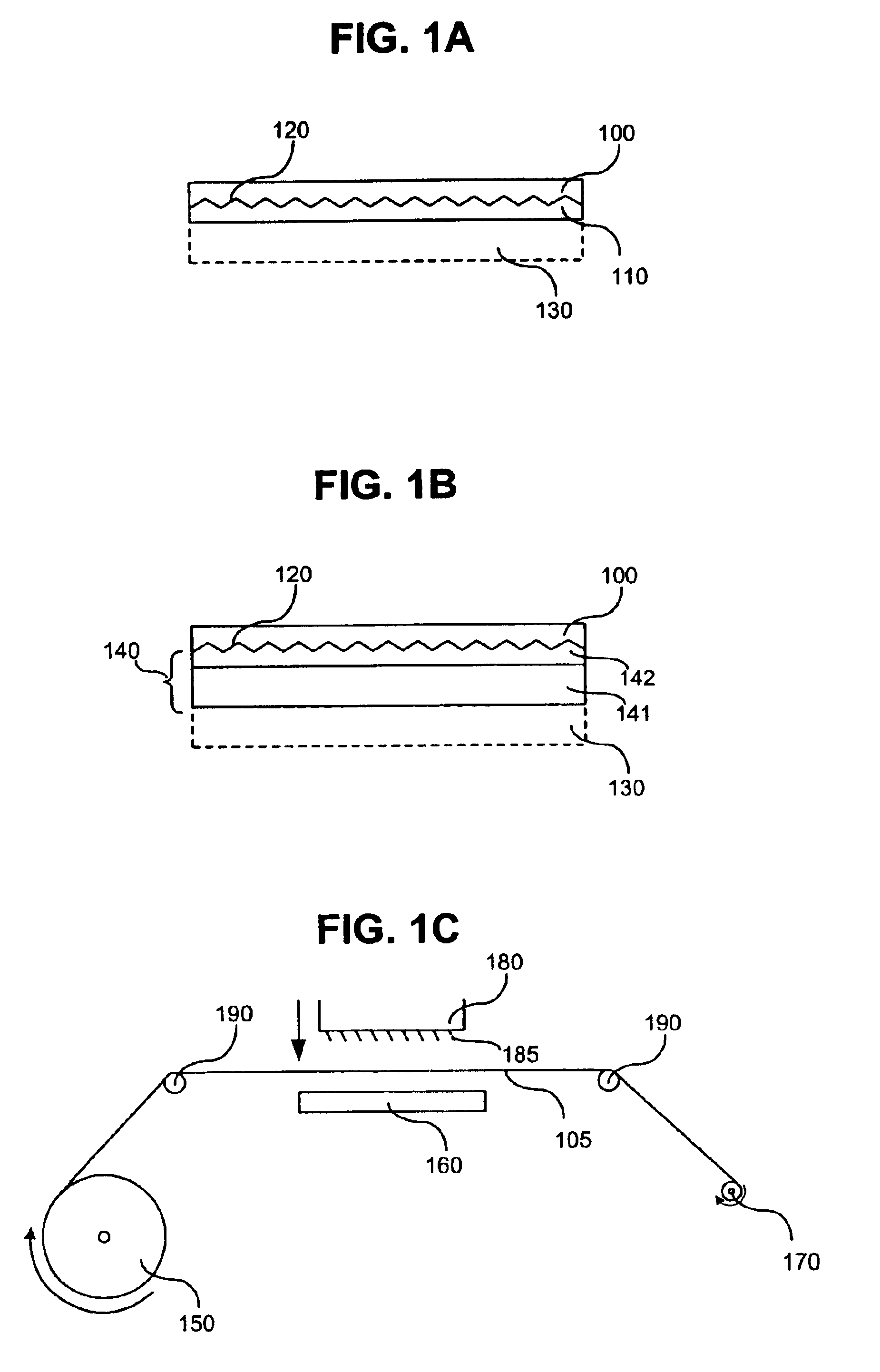
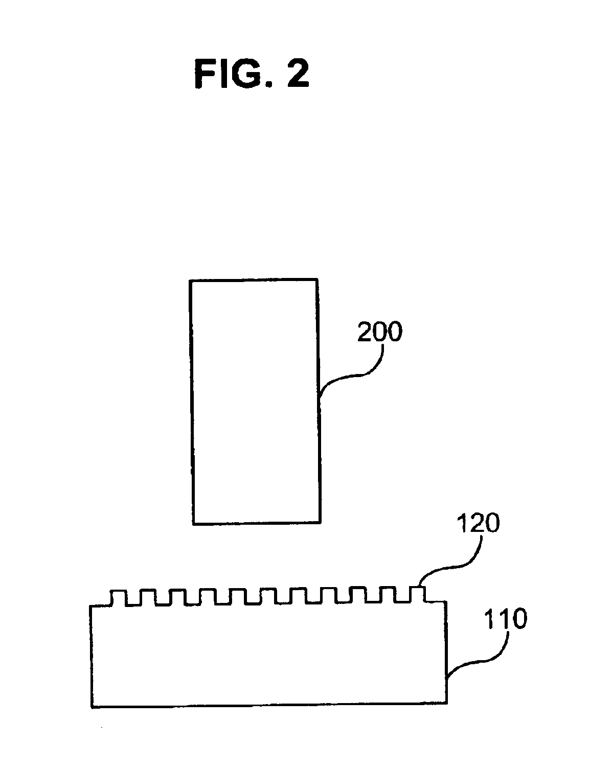
II. The Cleaning ApparatusA. Abrasive Substrate LayerB. Tacky Gel Layer / Material1. Silicone Base Resin2. Cross-linking Compound3. Orientation of Components

III. Method of Making the Cleaning Apparatus

IV. Method for Cleaning Probe Tips

I. Terminology of the Invention

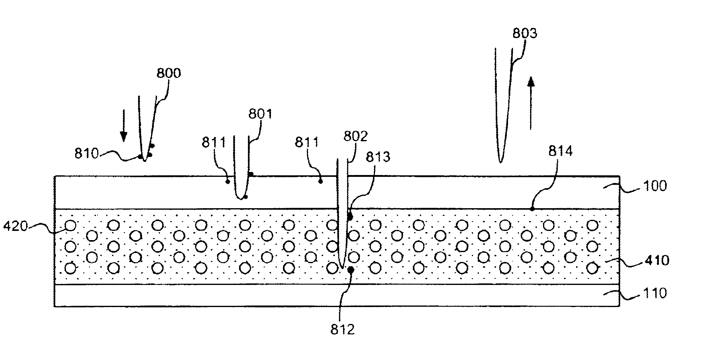
The term “probe tip” refers to the end portion of a probe element used for testing a semiconductor device.

The term “probe element” refers to, but is not limited to, tungsten needles, vertical probes, cobra probes, L-type probes, plunger probes, spring contact probes, and contact bump probes formed on a membrane.

The term “spring contact” (also referred to as a “contact spring” or as a “spring”) refers to, but is not limited to, any spring contact available now or in the future from FormFactor, Inc. a Delaware corporation. Any type of spring contact presently known can be used in according with the present invention. Examples of spring contacts that can be used with the present ...


PUM

PropertyMeasurementUnit
widthaaaaaaaaaa
widthaaaaaaaaaa
abrasiveaaaaaaaaaa

Abstract

A probe cleaning apparatus for cleaning a probe tip use to test semiconductors dies having an abrasive substrate layer an a tacky gel layer on top of the abrasive surface of the abrasive substrate layer. The probe tip is cleaned by passing it through the tacky gel layer so that it comes in contact with the abrasive surface of the abrasive substrate, moving the probe tip across the abrasive surface of the substrate layer, and then removing the probe tip from the successive layers of the cleaning apparatus. The probe tip emerges from the cleaning apparatus free from debris associated with testing the semiconductor dies.

Description

BACKGROUND OF THE INVENTION1. Field of the InventionThe present invention relates generally to probe cards that are used to perform tests on semiconductor devices. The present invention more particularly relates to the cleaning of probe elements that extend from such probe cards.2. Background ArtIndividual semiconductor (integrated circuit) devices (dies) are typically produced by creating several identical dies on a semiconductor wafer, using known techniques of photolithography, deposition, and the like. Generally, these processes are intended to create a plurality of fully-functional integrated circuit devices, prior to singulating (severing) the individual dies from the semiconductor wafer. In practice, however, certain physical defects in the wafer itself and certain defects in the processing of the wafer inevitably lead to some of the dies being “good” (fully-functional) and some of the dies being “bad” (non-functional). It is generally desirable to be able to identify which o...

Claims


Application Information

Patent Timeline
Patent Type & Authority Patents(United States)
IPC IPC(8): B08B1/00B08B7/00G01R1/067G01R3/00C08L83/05A47L25/00C08L83/07C08L83/08H01L21/304H01L21/66
CPCB08B1/00B08B7/0028C08G77/48Y10T428/24388G01R1/06711G01R3/00Y10T428/31663C08L83/04C08G77/06
Inventor KHANDROS, IGOR Y.ELDRIDGE, BENJAMIN N.FANG, TRELIANTMATHIEU, GAETAN L.GRUBE, GARY W.DRUSH, MICHAEL A.BUCKHOLTZ, CHRISTOPHER C.
Owner FORMFACTOR INC
Why Eureka
Try Eureka