Method of reducing in-trench smearing during polishing

a technology of in-trench smearing and polishing, which is applied in the direction of electrical equipment, basic electric elements, capacitors, etc., can solve the problems of inconvenient use, difficult subsequent wafer processing, and inability to provide consistent desired effects, so as to reduce the smearing of filling materials in the trench region and reduce the smearing of in-trench smearing

Inactive Publication Date: 2005-01-11
CABOT MICROELECTRONICS CORP
View PDF14 Cites 24 Cited by
  • Summary
  • Abstract
  • Description
  • Claims
  • Application Information

AI Technical Summary

Benefits of technology

The invention provides a method of reducing in-trench smearing during polishing. The method comprises providing a substrate comprising a first layer comprising an insulating material, a second layer comprising a filling material, and a plurality of field and trench regions. A polymeric material is infiltrated over the substrate, wherein the polymeric material fills the trench regions and covers the field regions. The polymeric material optionally is removed from the field regions, followed by baking of the substrate such that the polymeric material in the trench regions becomes recessed below the insulating material of the field regions. Whether or not the polymeric material is removed from the field regions, the substrate is then subjected to a temperature of about 100° C. or more for about 30 minutes or longer, such that during polishing of the substrate, smearing of the filling material in the trench regions is reduced as compared to polishing of the substrate under the same conditions except for subjecting the substrate to the temperature of about 100° C. or more for about 30 minutes or longer. When desirable, a layer of additional material can be deposited over the polymeric material such that it forms a layer over the polymeric material in the trench regions and the filling material in the field regions. The substrate is then polished to remove the polymeric material and filling material from the field regions of the substrate and to make the polymeric material in the trench regions substantially planar with or recessed below the insulating material of the field regions. If a layer of additional material is present, the additional material can be removed from the field regions of the substrate while the additional material in the trench regions is made to be substantially planar with the insulating material of the field regions.

Problems solved by technology

A problem associated with semiconductor processing typically involves smearing of the materials over the trench regions during polishing.
However, during polishing, materials can be undesirably smeared over portions of the substrate surface, sometimes partially or wholly covering the trench regions, making subsequent wafer processing difficult.
Most conventional schemes, however, do not provide consistent desired results.
Indeed, scratching, dishing, comer erosion, and / or smearing are common imperfections associated with many CMP processes when subsequent interconnect processing steps are required.

Method used


Image

  • Method of reducing in-trench smearing during polishing
  • Method of reducing in-trench smearing during polishing

Examples


Embodiment Construction

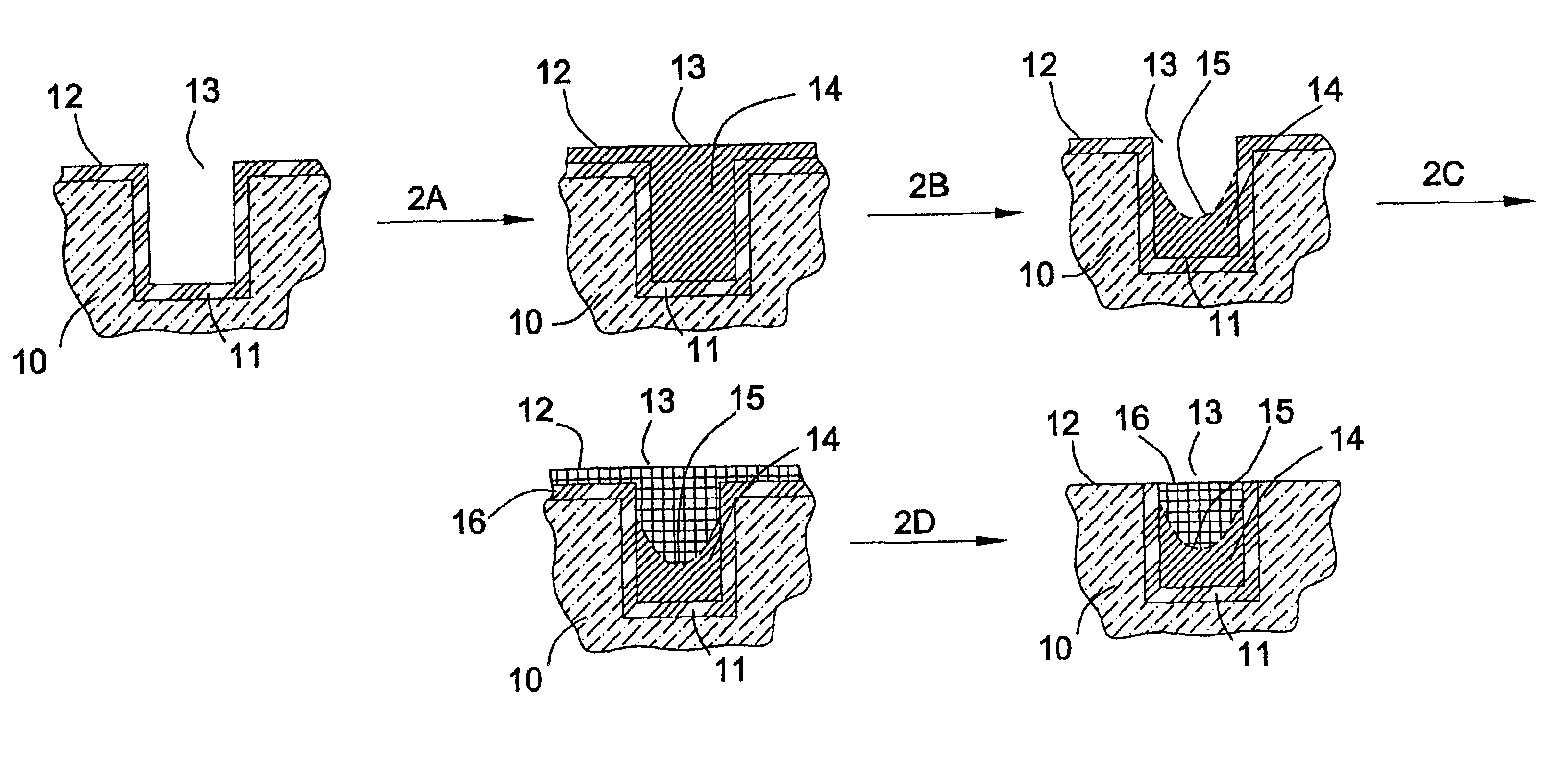
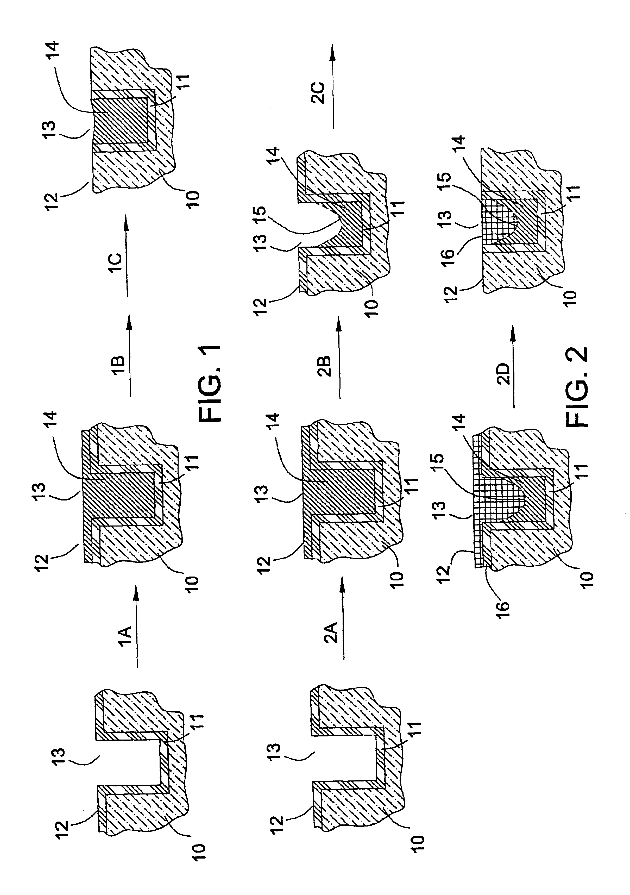
As illustrated in FIGS. 1 and 2, the invention provides a method of polishing a substrate comprising the following sequential steps: (a) providing a substrate comprising (i) a first layer comprising an insulating material (10), (ii) a second layer comprising a filling material (11) that differs from the insulating material, and (iii) a plurality of field (12) and trench regions (13), (b) infiltrating a polymeric material over the substrate (steps 1A and 2A), wherein the polymeric material (14) fills the trench regions and covers the field regions, (c) subjecting the substrate to a temperature of about 100° C. or more for about 30 minutes or longer, such that during polishing of the substrate, smearing of the filling material in the trench regions becomes reduced as compared to polishing of the substrate under the same conditions except for subjecting the substrate to the temperature of about 100° C. or more for about 30 minutes or longer (step 1B), and (d) polishing the substrate to...


PUM

PropertyMeasurementUnit
temperatureaaaaaaaaaa
dielectric constantaaaaaaaaaa
temperaturesaaaaaaaaaa

Abstract

The invention provides a method of reducing in-trench smearing during polishing. The method comprises providing a substrate comprising a first layer comprising an insulating material, a second layer comprising a filling material, and a plurality of field and trench regions. A polymeric material is infiltrated over the substrate, wherein the polymeric material fills the trench regions and covers the field regions. The polymeric material optionally is removed from the field regions, followed by baking of the substrate such that the polymeric material in the trench regions becomes recessed below the insulating material of the field regions. The substrate is then subjected to a temperature of about 100° C. or more for about 30 minutes or longer, such that during polishing of the substrate, smearing of the filling material in the trench regions is reduced as compared to polishing of the substrate under the same conditions except for subjecting the substrate to the temperature of about 100° C. or more for about 30 minutes or longer. When desirable, a layer of additional material can be deposited over the polymeric material such that it forms a layer over the polymeric material in the trench regions and the filling material in the field regions. The substrate is then polished to obtain a substantially planar surface.

Description

FIELD OF THE INVENTIONThis invention pertains to a method of polishing a substrate, particularly a substrate comprising a plurality of field and trench regions.BACKGROUND OF THE INVENTIONAs the size of integrated circuits is reduced and the number of integrated circuits on a chip increases, the components that make up the circuits must be positioned closer together in order to comply with the limited space available on a typical chip. Current research, therefore, is directed towards achieving a greater density of active components per unit area of a semiconductor substrate. In addition, the components must be oriented vertically by either building the devices up from the substrate surface or by burying the devices in trenches formed within the face of the semiconductor body. A trench capacitor, for example, has been used in dynamic random access memory (DRAM) cells and other circuits to try to further reduce the overall area of such devices.A problem associated with semiconductor pr...

Claims


Application Information

Patent Timeline
Patent Type & Authority Patents(United States)
IPC IPC(8): H01L21/02H01L21/762H01L21/70H01L21/321H01L21/3105
CPCH01L21/31053H01L21/76224H01L21/3212H01L21/31058H01L28/91
Inventor CHERIAN, ISAAC K.FEENEY, PAUL M.MOEGGENBORG, KEVIN J.
Owner CABOT MICROELECTRONICS CORP
Why Eureka
Try Eureka