Double-gated vertical junction field effect power transistor

a vertical junction field and power transistor technology, applied in transistors, electrical appliances, semiconductor devices, etc., can solve the problems of increasing current capability and reducing forward voltage drop, so as to facilitate a doubling of channel opening, reduce forward voltage drop, and increase current capability

Inactive Publication Date: 2005-01-11
RUTGERS THE STATE UNIV
View PDF3 Cites 36 Cited by
  • Summary
  • Abstract
  • Description
  • Claims
  • Application Information

AI Technical Summary

Benefits of technology

[0020]The double-gated structure facilitates a doubling of the channel opening within the low-voltage LJFET. Because a normally-off power switch current capability is limited by the low-voltage LJFET current capability, doubling the channel opening substantially increases the current capability and decreases the forward voltage drop.
[0021]The present invention provides a monolithic normally-off semiconductor power switch thereby advancing power switch technology in two important aspects. A buried epitaxial layer serves not only as one...

Problems solved by technology

Because a normally-off power switch current capability is limited by the low-voltage LJFET current capability,...

Method used


Image

  • Double-gated vertical junction field effect power transistor
  • Double-gated vertical junction field effect power transistor
  • Double-gated vertical junction field effect power transistor

Examples


Embodiment Construction

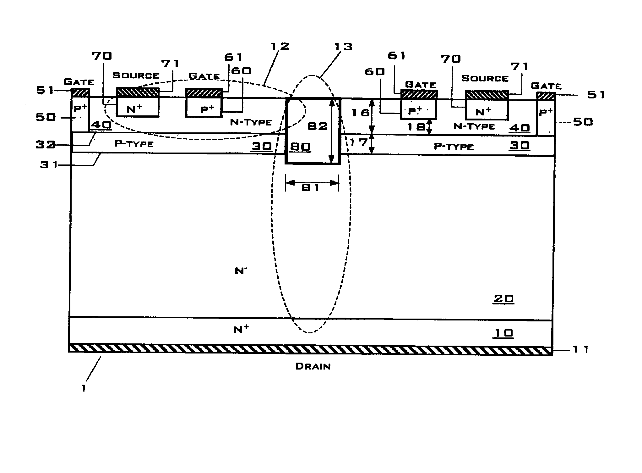
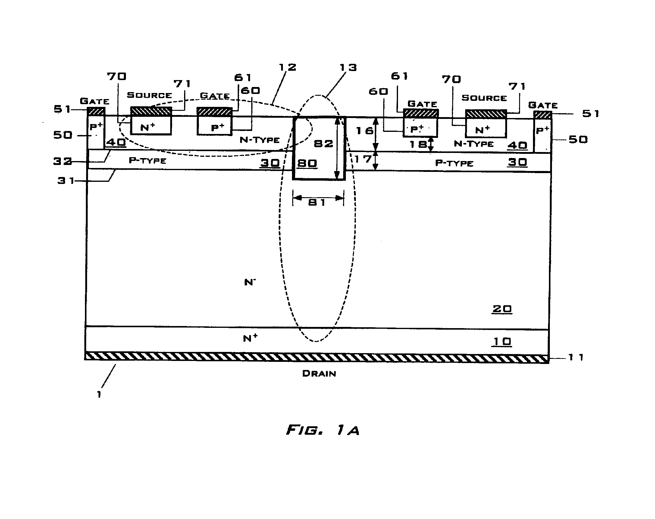
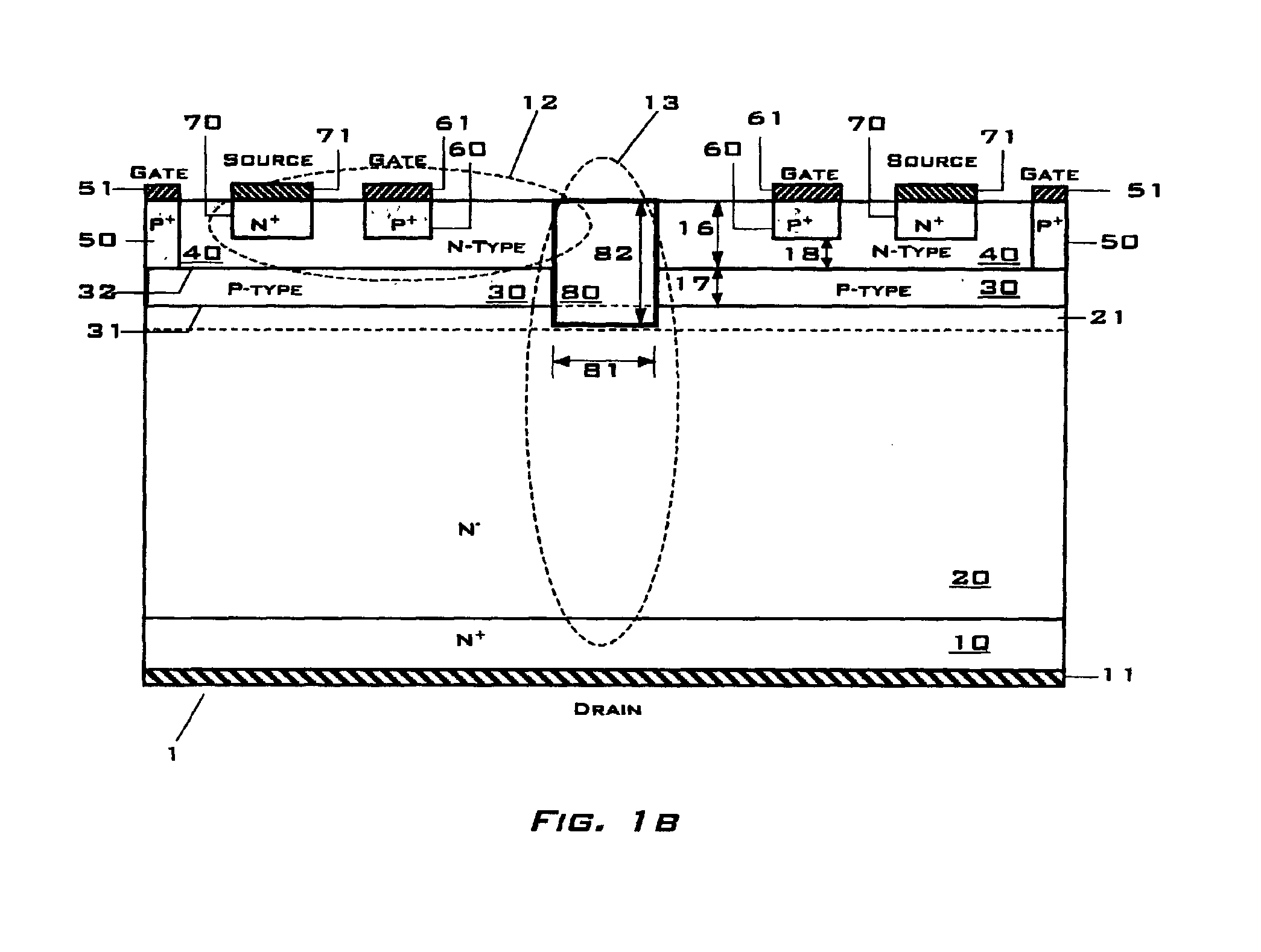
[0033]The present invention will now be described more fully hereafter with reference to the accompany drawings, in which preferred embodiments of the invention are described with SiC semiconductor serving as an example. The invention may, however, be embodied in many different forms for many different semiconductors including but not limited to GaN, AlGaN, GaP, AlGaAs, diamond, ZnO, and ZnO based materials among other semiconductors.

[0034]Referring to FIG. 1A, an enlarged sectional view is shown of a semiconductor power switch, referred to as a DG-VJFET 1, comprised of several layers. A planar-shaped substrate 10 composed of a heavily doped n-type semiconductor material known within the art is provided as the first layer and functionally facilitates ohmic contact formation. A lightly-doped yet thicker n-type drift layer 20 composed of material known within the art is likewise planar disposed and contacting the substrate 10. A planar disposed p-type layer 30 composed of material und...


PUM


Abstract

The present invention is a power semiconductor switch having a monolithically integrated low-voltage lateral junction field effect transistor (LJFET) controlling a high-voltage vertical junction field effect transistor (VJFET). The low-voltage LJFET conducting channel is double-gated by p+n junctions at opposite sides of the lateral channel. A buried p-type epitaxial layer forms one of the two p+n junction gates. A p+ region created by ion implantation serves as the p+ region for the second p+n junction gate. Both gates are electrically connected by a p+ tub implantation. The vertical channel of the vertical JFET is formed by converting part of the buried p-type epitaxial layer into n+ channel via n-type ion implantation.

Description

NON-PROVISIONAL PATENT APPLICATIONCROSS REFERENCE TO RELATED APPLICATIONS[0002]This application claims benefit under 35 U.S.C. 119(e) from U.S. Provisional Application No. 60 / 348,232 filed on Nov. 9, 2001.FEDERALLY SPONSORED RESEARCH OR DEVELOPMENT[0003]None.BACKGROUND OF THE INVENTION[0004]1. Field of the Invention[0005]The present invention generally relates to a power semiconductor switch. Specifically, the invention is a power switch in which a double-gated, normally-off, low-voltage lateral junction field effect transistor (LJFET) is employed to control a normally-on, high-voltage vertical junction field effect transistor (VJFET).[0006]2. Background[0007]An ideal power semiconductor switch possesses important features, capabilities, and characteristics. A normally-off feature is significantly important to power systems since it avoids the dangers and design complications of normally-on designs, especially at high power levels. A voltage control capability is a widely desired ad...

Claims


Application Information

Patent Timeline
IPC IPC(8): H01L29/66H01L29/423H01L29/40H01L29/808
CPCH01L29/8083H01L29/42316
Inventor ZHAO, JIAN HUI
Owner RUTGERS THE STATE UNIV
Why Eureka
Try Eureka