Premolded cavity IC package

a technology of integrated circuits and pre-molded cavities, which is applied in the direction of electrical equipment, semiconductor devices, semiconductor/solid-state device details, etc., can solve the problems of inability to support the inner lead of these packages, cost prohibitive packages, and inconvenient packaging

Inactive Publication Date: 2005-01-11
UTAC HEADQUARTERS PTE LTD
View PDF17 Cites 82 Cited by
  • Summary
  • Abstract
  • Description
  • Claims
  • Application Information

AI Technical Summary

Benefits of technology

In one aspect of the invention, an air cavity in the interior of the package body and the clamped inner portion

Problems solved by technology

However, these packages are cost prohibitive.
Again, these packages are cost prohibitive as they employ a substrate rather than a less-expensive leadframe.
However, the inner leads of these packages are not

Method used


Image

  • Premolded cavity IC package
  • Premolded cavity IC package
  • Premolded cavity IC package

Examples


Embodiment Construction

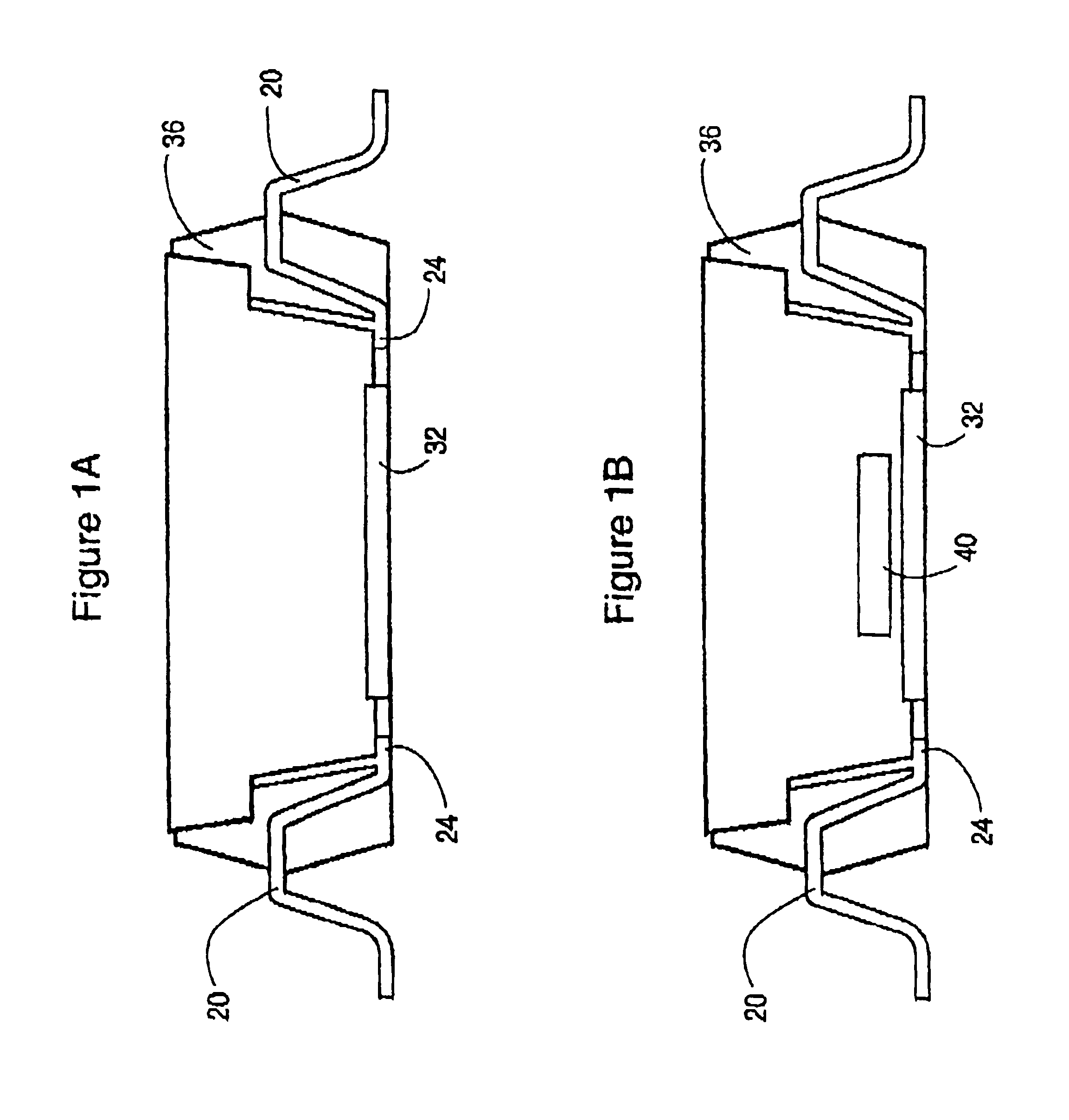
With reference to FIGS. 1A to 1E, each of a plurality of formed leads 20 is supported by clamping an interior portion 24 of the leads 20 between a top and a bottom mold cavity in an appropriately shaped mold (not shown). A die attach pad 32 is held at the four corners by tie bars on a leadframe.

A package body 36 is then molded in the mold such that the formed leads 20 extend from an interior of the package body 36 to an exterior thereof, as best shown in FIG. 1A. The package body 36 is then removed from the mold.

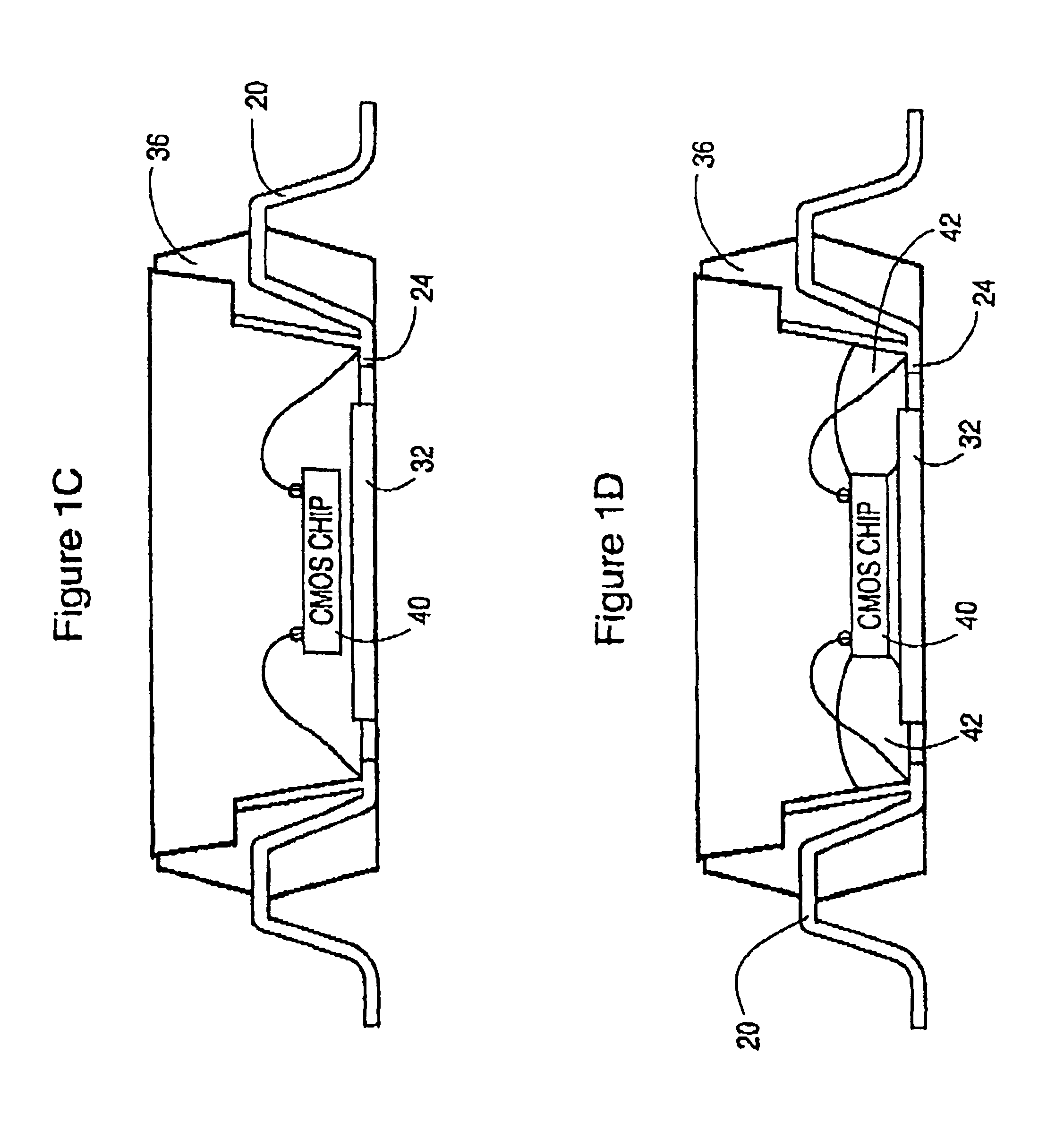
Next, a semiconductor die 40 is fixed to the die attach pad 32 using conventional techniques, for example, using epoxy or film, as shown in FIG. 1B. This is followed by standard wire bonding of the interior portion 24 of the leads 20 to the semiconductor die 40, as shown in FIG. 1C.

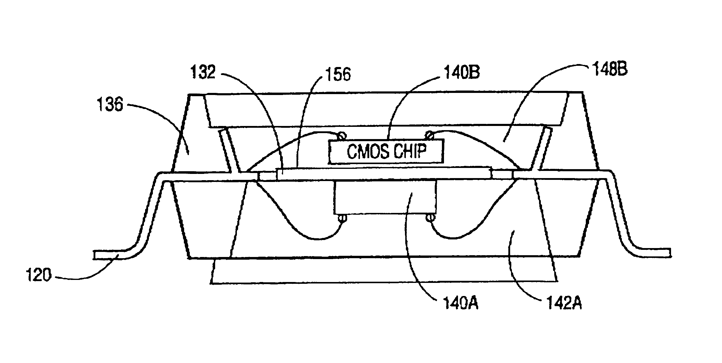
Referring now to FIG. 1D, a fill material (glob top fill) 42 is added to the cavity, generally between the semiconductor die 40 and the package body 36. The glob top fill 42 covers the interior po...


PUM


Abstract

A process for fabricating a cavity-type integrated circuit package. The process includes: supporting an interior portion of each of a plurality of leads, in a mold; supporting a die attach pad in said mold; molding a package body in said mold such that said leads extend from an interior cavity of said package body to an exterior thereof; mounting a semiconductor die to said die attach pad; wire bonding various ones of said leads to said semiconductor die; adding a fill material for covering at least a surface of said interior portion of said leads; and mounting a lid on said package body for enclosing said die in said cavity of said package body.

Description

FIELD OF THE INVENTIONThe present invention relates in general to integrated circuit packaging, and more particularly to an improved process for fabricating a premolded cavity integrated circuit package that includes a feature to inhibit mold contamination of the inner lead bonding area.BACKGROUND OF THE INVENTIONCavity-type IC packages are useful in imaging devices such as CMOS imaging or CCD display applications for still or video cameras. The package includes a die at the base of a cavity and a clear lid epoxied on top. The use of a cavity-type IC package is advantageous for high frequency applications as the gold interconnect wires between the die attach pad and the contacts span an air gap rather than travelling through mold compound. The air has a lower dielectric constant than the mold compound and therefore the electrical impedance of the gold wire is much lower when the wire runs through air rather than through the mold compound. Thus signal distortion at high frequencies i...

Claims


Application Information

Patent Timeline
IPC IPC(8): H01L23/495H01L23/02H01L23/10H01L23/48H01L23/16H01L23/24
CPCH01L23/10H01L23/49575H01L23/24H01L2224/73265H01L2224/48465H01L2224/32245H01L2224/45144H01L24/49H01L24/48H01L2924/3011H01L2924/1532H01L2924/01079H01L2224/49109H01L2224/48247H01L2224/48091H01L2924/00014H01L2924/00H01L24/45H01L2924/14H01L2924/181H01L2924/00015H01L2224/05599H01L2924/00012
Inventor THAMBY, LABEEB SADAKMCLELLAN, NEILWONG, HUGO CHI WAICHOW, WILLIAM LAP KEUNG
Owner UTAC HEADQUARTERS PTE LTD
Why Eureka
Try Eureka