Probe card apparatus and electrical contact probe having curved or sloping blade profile

Inactive Publication Date: 2005-01-11
INNOTECH CORP
View PDF21 Cites 54 Cited by
  • Summary
  • Abstract
  • Description
  • Claims
  • Application Information

AI Technical Summary

Benefits of technology

By this structure, as the probe is brought into pressure contact with the electrode portion as described above, the hooked stylus portion cuts into the insulating film. As the probe slides over the electrode portion, the hooked stylus portion cuts and slits the insulating film and reaches the electrode portion positioned, below the insulating film, surely establishing electrical co

Problems solved by technology

This hinders satisfactory conduction between probe 101 and pad electrode 5, making an electrical test impossible.
The time required for mainte

Method used


Image

  • Probe card apparatus and electrical contact probe having curved or sloping blade profile
  • Probe card apparatus and electrical contact probe having curved or sloping blade profile
  • Probe card apparatus and electrical contact probe having curved or sloping blade profile

Examples


Example

First Embodiment

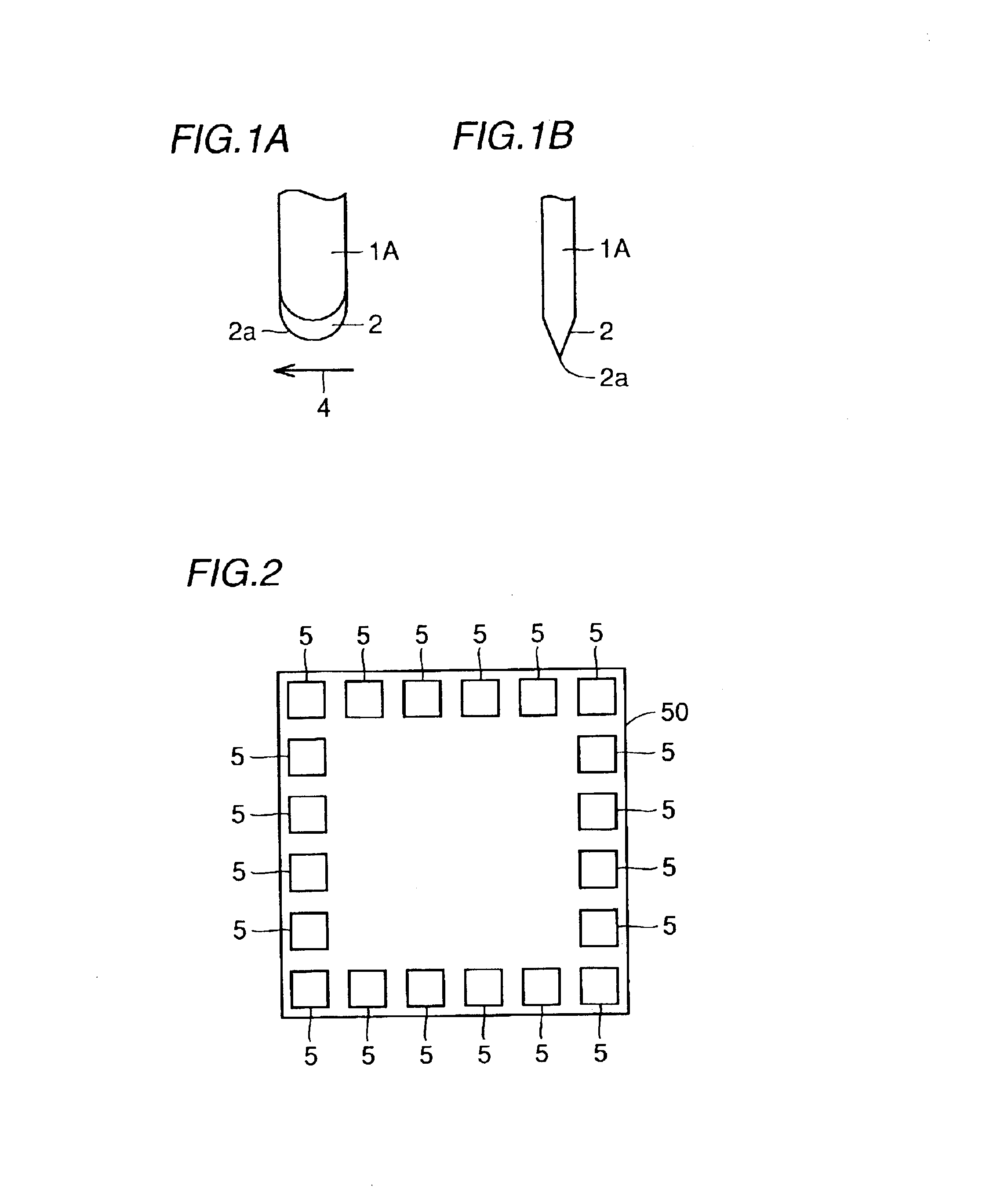
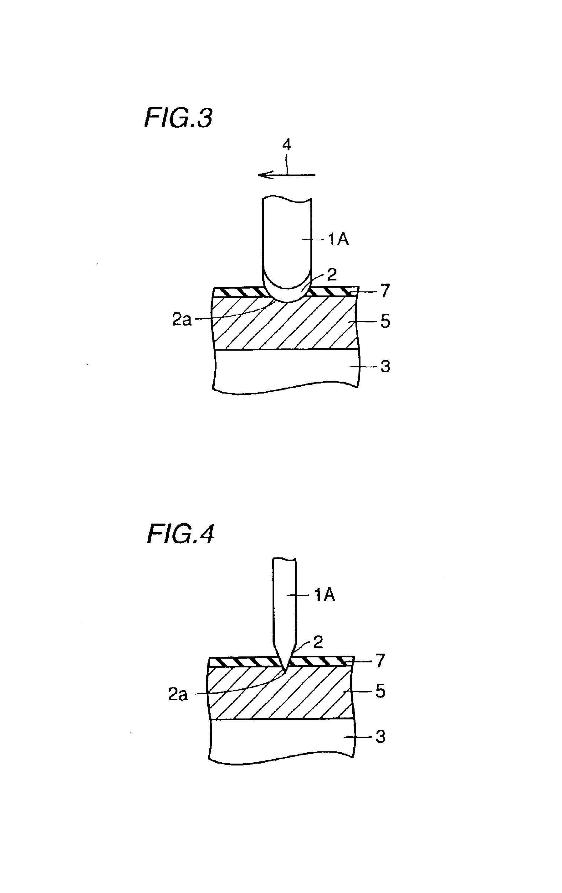
The probe in accordance with the first embodiment of the present invention will be described. Referring to FIGS. 1A and 1B, probe 1A in accordance with the first embodiment of the present invention has a cutting blade portion 2 at the tip end portion that is brought into contact with a pad electrode. Cutting blade portion 2 has a cutting edge 2a, which is in one plane parallel to the direction of sliding (arrow 4) relative to the pad electrode, when the cutting blade is brought into contact with the pad electrode.

Particularly, cutting edge 2a curves as seen in FIG. 1A so that it becomes closer to the pad electrode portion from the front side to the rear side, along the direction of progress, at the front edge in the direction of progress when it slides over the pad electrode.

Next, a probe card in accordance with the first embodiment of the present invention that includes probe 1A will be described. The probe card is similar to the probe card shown in FIG. 18, except ...

Example

Second Embodiment

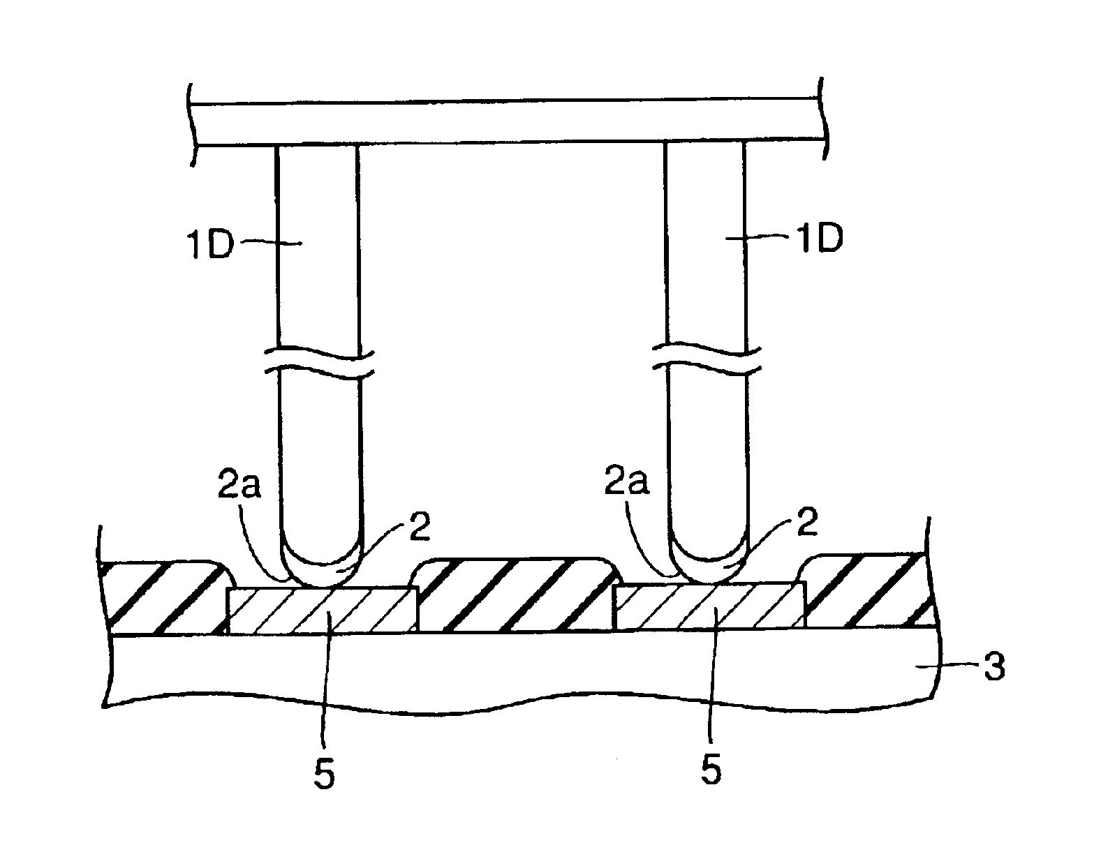
In the first embodiment, a probe card having a plurality of probes arranged radially has been described as an example. Such a probe card is applied when the pad electrodes formed on the semiconductor chip are arranged relatively regularly, as shown in FIG. 2, for example.

In the present embodiment, a probe card will be described that can be applied to such a semiconductor chip 51 on which pad electrodes 5 are arranged relatively irregularly, as shown in FIG. 13, for example.

It is physically difficult to electrically test the semiconductor chip 51 on which pad electrodes 5 are arranged irregularly by means of a probe card having a plurality of probes arranged radially. Therefore, the probe card of the present embodiment has a plurality of probes 1D arranged to prick each pad electrode 5 approximately vertically. Further, all the planes including the cutting edges 2a at the tip end of probe 1D are arranged approximately parallel to one direction. The direction is appro...


PUM


Abstract

A probe (1A) has a cutting blade portion (2) at a tip end that is brought into contact with a pad electrode (5). The cutting blade has a cutting edge that is in a plane parallel to the direction of sliding of the blade over a pad electrode, when the edge is brought into contact with the electrode. The cutting edge (2a) has a sloping or curved shape that comes closer to the electrode from the front side to the rear side of the blade along the direction of sliding. Thus, as the cutting edge (2a) cuts into an insulating coating (7) formed on the surface of the electrode, the probe ensures satisfactory electrical conduction between the probe (1A) and the electrode because it cuts through the coating without causing swarfs.

Description

TECHNICAL FIELDThe present invention relates to a probe card apparatus and a probe used therefor, and more specifically, to a probe card apparatus and a probe used therefor providing satisfactory electrical contact with a prescribed electrode portion formed on a semiconductor chip and the like, when a plurality of semiconductor chips formed on a silicon wafer is subjected to an electrical test such as a circuit test, in the form of a wafer, or when circuit elements such as liquid crystal display panels (LCD) and the like are subjected to electrical circuit test.BACKGROUND ARTA plurality of pad electrodes mainly consisting of aluminum or the like are arranged and formed on a surface of a semiconductor chip, a liquid crystal display panel or the like (hereinafter referred to as an “object of measurement”). For example, when a semiconductor chip in the form of a wafer is to be electrically tested, a probe card for electrically connecting each of the pad electrodes with a prescribed mea...

Claims


Application Information

Patent Timeline
IPC IPC(8): G01R1/067G01R1/073H01L21/66
CPCG01R1/06738G01R1/073
Inventor YOSHIDA, MINORUOHASHI, SEIICHI
Owner INNOTECH CORP
Why Eureka
Try Eureka