Thin film acoustic resonator and method of producing the same

a thin film acoustic resonator and bulk technology, applied in the direction of generator/motor, mechanical vibration separation, instruments, etc., can solve the problems of difficult to increase the achievement amount of final products, difficult to increase the insufficient crystal quality of piezoelectric thin films, etc., to achieve remarkable improvement

Inactive Publication Date: 2005-01-11
MEMS SOLUTIONS INC
View PDF15 Cites 222 Cited by
  • Summary
  • Abstract
  • Description
  • Claims
  • Application Information

AI Technical Summary

Benefits of technology

The inventors have discovered that the temperature stability of resonance frequencies can be improved with keeping high electromechanical coupling coefficient and high acoustic quality factor by forming electrodes on both the surfaces of a piezoelectric thin film which is mainly formed of AlN, the electrodes being mainly formed of molybdenum (Mo) that has larger elastic modulus than general electrode materials such as gold, platinum, aluminum, copper, etc. and remarkably small thermal elasticity loss, and further forming an insulating layer mainly containing silicon oxide (SiO2) or silicon nitride (Si3N4) having a temperature coefficient of resonant frequency whose sign is different from the temperature coefficient of resonant frequency of the piezoelectric thin film while the insulating layer is contained in the vibration portion, and have implemented the present invention on the basis of this discovery. Further, the inventors have also discovered that high-performance FBAR having high electromechanical coupling coefficient and high acoustic quality factor and remarkably excellent temperature stability can be implemented by setting the thickness of each layer so as to satisfy 0.1≦t′ / t≦0.5, preferably 0.2≦t′ / t≦0.4 wherein the thickness of the piezoelectric thin film mainly formed of aluminum nitride is represented by t and the thickness of the insulating layer mainly formed of silicon oxide or silicon nitride (when there are plural insulating layers, “thickness” means the total thickness of the respective insulating layers) is represented by t′.
Further, according to the present invention, there are provided a VCO (voltage control oscillator), a filter and a transmission / reception duplexer which are constructed by using the piezoelectric thin film resonator described above, and the characteristics can be remarkably improved at high frequencies of 1 GHz or more in these devices.

Problems solved by technology

However, the hole thus formed so as to penetrate through the wafer makes the wafer very fragile and easily breakable.
Further, if wet etching using KOH is carried out at an etching inclination angle of 54.7 degrees with respect to the surface of the substrate, it would be difficult to increase the achievement amount of final products, that is, to increase the yield of FBAR / SBAR on wafer.
The 0.1 μm-order RMS variation is an insufficient surface roughness for the surface on which piezoelectric thin film for a thin film bulk acoustic resonator is formed.
However, the crystal is grown in various directions due to the effect of various unevenness on the rough surface, so that the crystal quality of the piezoelectric thin film achieved is not sufficient.
However, this method has many problems.
That is, since a metal layer forms a parasitic capacitor which degrades the electrical performance of the filter, it cannot be used as the layer of the Bragg reflection mirror.
Therefore, selection of materials usable for the Bragg reflection mirror is restricted.
Further, in this method, stress applied to each layer must be controlled with high precision, and thus the manufacturing process is complicated.
Further, it is difficult to form a viahole penetrating a large number of layers such as the number of 10 to 14, and thus the acoustic resonators achieved according to this method are unfavorable to integration with other active elements.
However, there is no specific description on enhancement of adhesion force to silicon wafer, etc. serving as a substrate.
However, when no Ti adhesion layer is formed and only the Au electrode layer is solely formed, the adhesion force between the substrate and the Au electrode layer is insufficient, and occurrence of exfoliation, etc. remarkably reduces the durability of the thin film bulk acoustic resonator under operation.
However, there have not yet achieved any thin film bulk acoustic resonator and any thin film filter which can exhibit sufficient performance in GHz band.

Method used


Image

  • Thin film acoustic resonator and method of producing the same
  • Thin film acoustic resonator and method of producing the same
  • Thin film acoustic resonator and method of producing the same

Examples


example 1

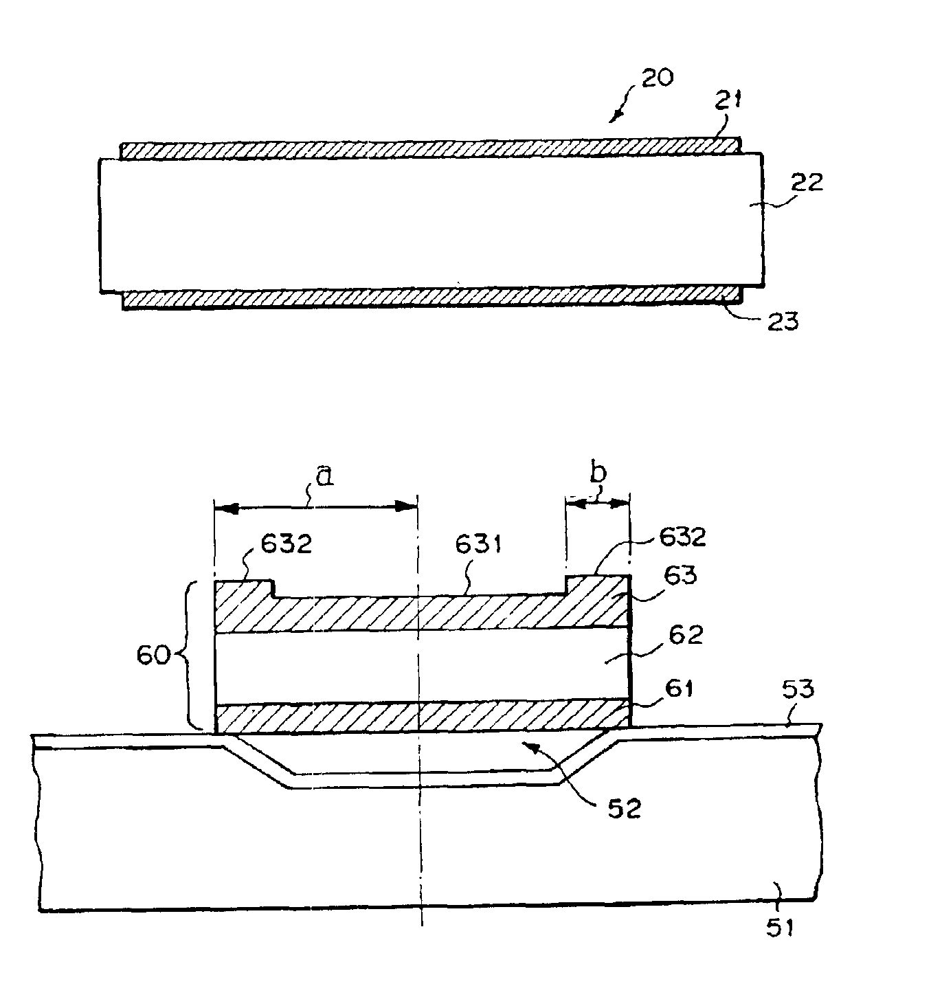
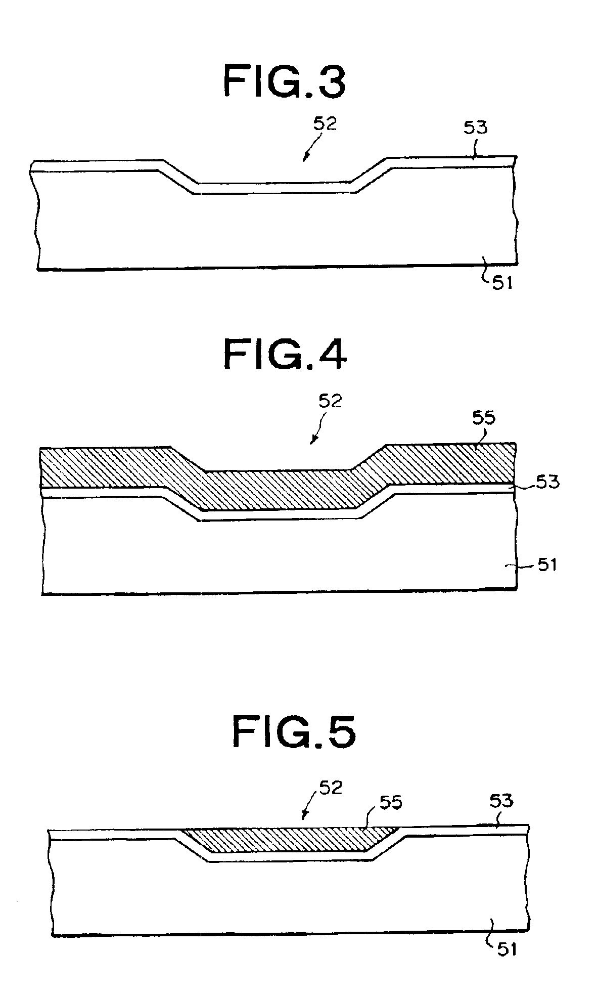
A thin film bulk acoustic resonator was manufactured in the manner as shown in FIGS. 3 to 8.

First, the surface of a Si wafer 51 was coated with a Pt / Ti protection film, and the protection film was etched to have a predetermined pattern for formation of a pit or cavity or recess, thereby forming a mask for etching the Si wafer 51. Thereafter, wet etching was carried out by using the Pt / Ti pattern mask thus formed to form a pit or cavity or recess of 20 μm in depth and 150 μm in width. The etching was carried out with KOH water solution of 5% by weight at a liquid temperature of 70° C. Alternatively, the depth of the pit may be set to 3 μm.

Thereafter, the Pt / Ti pattern mask was removed, and a SiO2 layer 53 of 1 μm in thickness was formed on the surface of the Si wafer 51 by thermal oxidation, thereby achieving such a structure that the pit 52 is formed in the substrate comprising the Si wafer 51 and the SiO2 layer 53.

Subsequently, as shown in FIG. 4, a PSG sacrificial layer 55 of 30 μ...

example 2

An acoustic resonator was manufactured in the same manner as EXAMPLE 1 except that AlN film was used as the piezoelectric film 62 in place of the ZnO film. That is, the piezoelectric layer 62 comprising an AlN film of 1.2 μm in thickness was formed on the lower electrode 61. The formation of the AlN film was carried out by using the RF magnetron sputtering method at a substrate temperature of 400° C. under the condition that Al was used as sputtering target and the mixture gas of Ar and N2 was used as sputter gas. The surface roughness of the AlN film thus formed was measured, and the result was that the RMS variation of the height was equal to 14 nm which was not more than 5% of the film thickness. With respect to the surface of the upper electrode 63, the waviness height at the measurement length of 150 μm was measured, so that the it was equal to 0.2 μm which was not more than 25% of the thickness of the piezoelectric layer 62 and also not more than 0.5% of the measurement length...

example 3

A thin film bulk acoustic resonator was manufactured in the same manner as shown in FIGS. 3 to 5 and FIGS. 9 to 10.

First, a structure shown in FIG. 5 was achieved in the same manner as EXAMPLE 1. However, the surface of the PSG sacrificial layer 55 remaining in the pit 52 was polished with slurry containing fine polishing particles so that the RMS variation of the height of the surface was equal to 5 nm.

Subsequently, as shown in FIG. 9, the insulating layer 54 comprising a SiO2 film of 500 nm in thickness was formed on the substrate by the CVD method so that the surface of the PSG sacrificial layer 55 was also covered by the insulating layer 54. The surface roughness of the insulating layer 54 thus formed was measured, so that the RMS variation of the height was equal to 10 nm.

Subsequently, as in the case of EXAMPLE 1, the lower electrode 61 comprising a Mo film was formed on the insulating layer 54 as shown in FIG. 10. The surface roughness of the Mo film thus formed was measured, ...


PUM

PropertyMeasurementUnit
thicknessaaaaaaaaaa
heightaaaaaaaaaa
heightaaaaaaaaaa

Abstract

A pit (52) is formed in a substrate comprising a silicon wafer (51) on a surface of which a silicon oxide thin layer (53) is formed. A sandwich structure (60) comprising a piezoelectric layer (62) and lower and upper electrodes (61, 63) joined to both surfaces of the piezoelectric layer is disposed so as to stride over the pit (52). The upper surface of the lower electrode (61) and the lower surface of the piezoelectric layer (62) joined to the upper surface of the lower electrode are treated so that the RMS variation of the height thereof is equal to 25 nm or less. The thickness of the lower electrode (61) is set to 150 nm or less. According to such a structure, there is provided a high-performance thin film bulk acoustic resonator which are excellent in electromechanical coupling coefficient and acoustic quality factor.

Description

This application claims priority benefits from Japanese Patent Application No. 2001-141845 filed May 11, 2001 and Japanese Patent Application No. 2001-141848 filed May 11, 2001 and Japanese Patent Application No. 2001-182194 filed Jun. 15, 2001.TECHNICAL FIELDThe present invention relates to a thin film bulk acoustic resonator using an electroacoustic effect of a piezoelectric thin film, and more particularly to a thin film bulk acoustic resonator usable as a constituent element of a filter for electronic circuits of communication equipment and a method of producing the same.Further, the present invention relates to a device using a piezoelectric thin film used in a broad field such as a thin film oscillator, a thin film VCO (Voltage Control Oscillator), a thin film filter, a duplexer, various kinds of sensors, etc. used in mobile communication equipment or the like.BACKGROUND TECHNIQUEIn order to meet the need of reducing the cost and size of electronic equipment, an effort of redu...

Claims


Application Information

Patent Timeline
Patent Type & Authority Patents(United States)
IPC IPC(8): B06B1/06G10K11/04G10K11/00H03H3/02H03H9/17H03H9/00H03H9/05H03H9/56H03H3/00H03H9/125H03H9/13H04R19/02G10L25/90H01L41/09H01L41/22H01L41/313H03H9/02H03H9/58H04R31/00
CPCB06B1/0644H03H3/02H03H9/02094H03H9/02102H03H9/02149H03H9/173H03H9/174H03H9/562H03H9/564H03H9/585H03H9/587G10K11/04Y10T29/49155H03H2003/021H03H2003/0428Y10S977/888Y10T29/42H03H9/54
Inventor YAMADA, TETSUONAGAO, KEIGOHASHIMOTO, CHISEN
Owner MEMS SOLUTIONS INC
Why Eureka
Try Eureka