Back contact solar battery and preparing method thereof

A technology for a solar cell and a manufacturing method, which is applied in the field of solar cells, can solve the problems of high cost, complicated manufacturing process, shortened life of a silicon substrate body, etc., and achieves the effect of reducing manufacturing cost and simplifying manufacturing method.

Active Publication Date: 2013-10-09
YINGLI GRP +2
View PDF5 Cites 41 Cited by
  • Summary
  • Abstract
  • Description
  • Claims
  • Application Information

AI Technical Summary

Problems solved by technology

[0004] However, the manufacturing process of traditional back-contact solar cells is complicated, the cost is high, and multiple high-temperatu

Method used


Image

  • Back contact solar battery and preparing method thereof
  • Back contact solar battery and preparing method thereof
  • Back contact solar battery and preparing method thereof

Examples


Embodiment 1

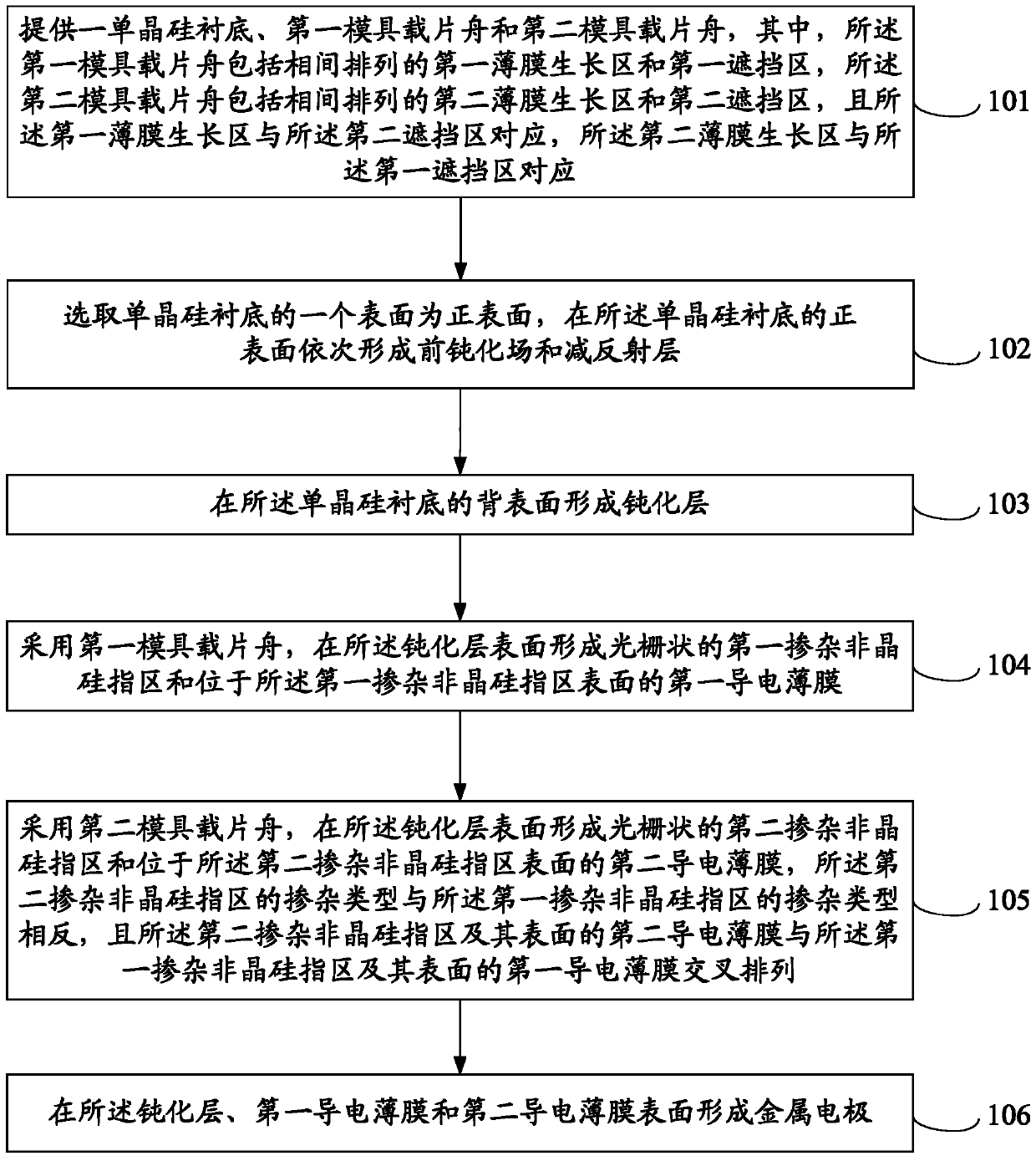
[0043] This embodiment provides a method for fabricating a back contact solar cell, such as figure 1 shown, including the following steps:

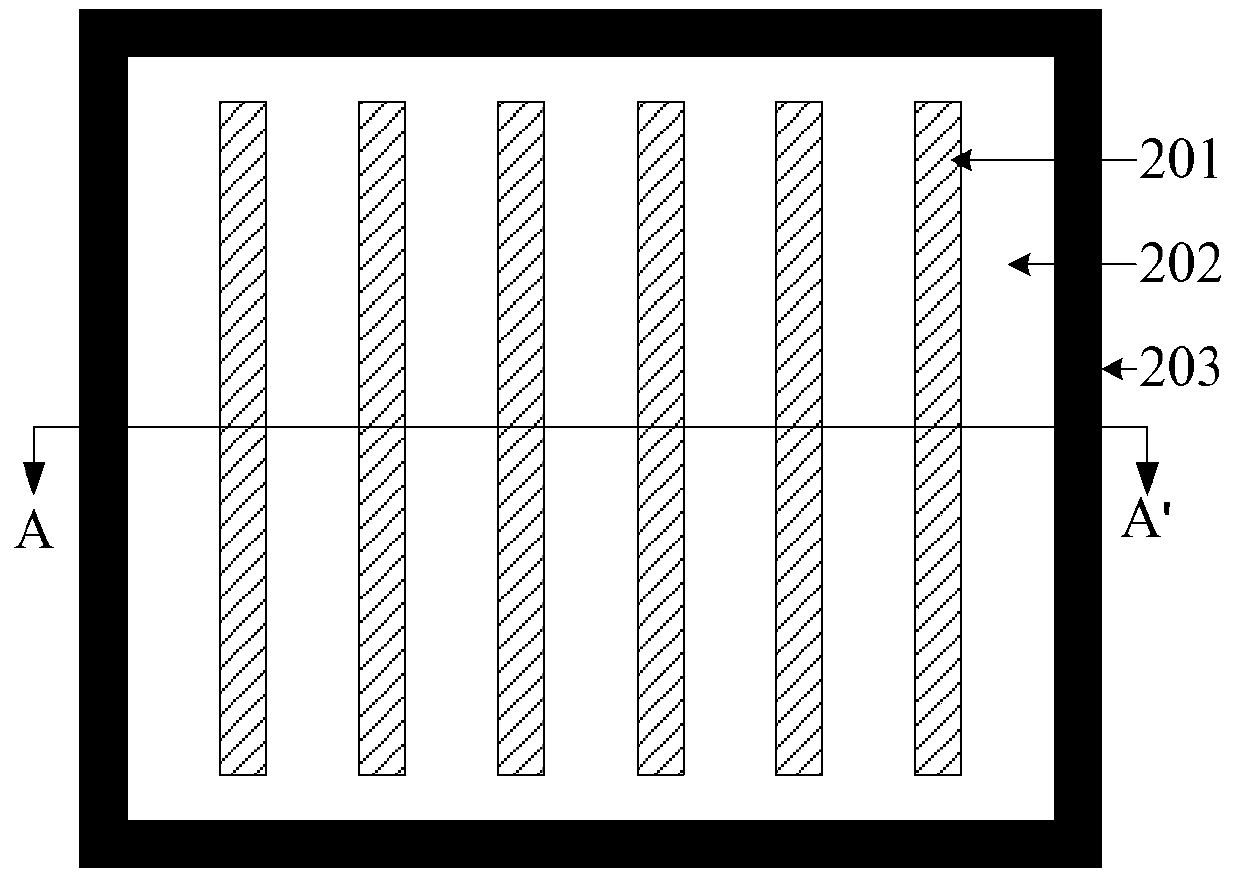
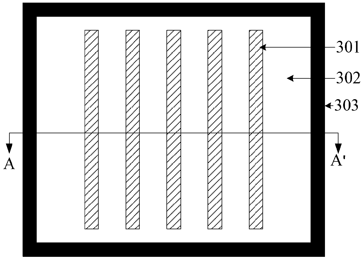
[0044] Step 101: Provide a single crystal silicon substrate, the first mold carrier boat 20 and the second mold carrier boat 30, wherein the top view of the first mold carrier boat 20 is as follows figure 2 As shown, the top view of the second mold carrier boat 30 is as image 3 As shown, while the cross-sectional view of the first mold carrier boat 20 and the second mold carrier boat 30 along AA' is as Figure 4 shown.

[0045] Such as figure 2 As shown, the first mold carrier boat 20 includes first thin film growth regions 201 and first shielding regions 202 arranged alternately, and the first thin film growth region 201 is a hollowed-out region located between the first shielding regions 202 . Such as image 3 As shown, the second mold carrier boat 30 also includes a second film growth region 301 and a second shielding region 30...

Embodiment 2

[0072] This embodiment provides a back contact solar cell, the back contact solar cell is formed by the manufacturing method described in Embodiment 1, such as Figure 12 As shown, the back contact solar cell includes: a single crystal silicon substrate 1201; a passivation layer 1205 located on the back surface of the single crystal silicon substrate 1201; a first doped amorphous silicon substrate located on the surface of the passivation layer 1205 The silicon finger region 1206 and the first conductive film 1207 on its surface; the second doped amorphous silicon finger region 1206 and the first conductive film 1207 on its surface are arranged crosswise on the surface of the passivation layer 1205 The doped amorphous silicon refers to the region 1208 and the second conductive film 1209 on its surface.

[0073] Wherein, the thickness d of the first doped amorphous silicon finger region 1206 and the second doped amorphous silicon finger region 1208 is 1 3nm to 30nm, including ...


PUM

PropertyMeasurementUnit
Thicknessaaaaaaaaaa
Thicknessaaaaaaaaaa
Gapaaaaaaaaaa

Abstract

The invention provides a back contact solar battery and a preparing method of the back contact solar battery. The preparing method of the back contact solar battery includes the steps of providing a first mould slide boat and a second mould slide boat, wherein the first mould slide boat comprises first film growing areas and first shielding areas which are distributed alternatively, and the second mould slide boat comprises second film growing areas and second shielding areas which are distributed alternatively, the first film growing areas correspond to the second shielding areas, and the second film growing areas correspond to the first shielding areas. First doped amorphous silicon indication areas and second doped amorphous silicon indication areas are formed on the surfaces, with passivated layers, of monocrystalline silicon substrates through the mould slide boats, wherein the first doped amorphous silicon indication areas and the second doped amorphous silicon indication areas are opposite in doping type and crossed in distribution. By means of the preparing method, a fork structure of a back field of the back contact solar battery is achieved simply at low cost, additional manufacturing process of forming the passivated layers is needless, and the preparing method of the back contact solar battery is simplified.

Description

technical field [0001] The invention belongs to the field of solar cells, in particular to a back-contact solar cell and a manufacturing method thereof. Background technique [0002] Solar power generation technology is an important field of new energy development. In order to increase unit power generation, it is very important to use solar cells with high energy conversion efficiency. The main electrical parameters that determine the energy conversion efficiency of solar cells include short-circuit current, open-circuit voltage, and fill factor. Among them, the short-circuit current corresponds to the optical shading loss of the solar cell, the open-circuit voltage represents the recombination loss of the solar cell, and the fill factor represents the electrical properties of the solar cell. loss. That is, if one wants to improve the energy conversion efficiency of solar cells, breakthroughs can be found in three aspects of reducing optical shading loss, recombination los...

Claims


Application Information

Patent Timeline
IPC IPC(8): H01L31/18H01L31/0224
CPCH01L31/0747H01L31/022441Y02E10/50
Inventor 陈剑辉李锋沈燕龙赵文超李高非胡志岩熊景峰
Owner YINGLI GRP
Why Eureka
Try Eureka