

Method of forming silicon oxide layer
a silicon oxide layer and silicon oxide technology, applied in the direction of coatings, liquid surface applicators, chemical vapor deposition coatings, etc., can solve the problems of complex process, difficult to form uniform silicon oxide layers with good reproducibility, and non-uniform thickness of oxide layers, etc., to achieve excellent properties
- Summary
- Abstract
- Description
- Claims
- Application Information
AI Technical Summary
Benefits of technology
Problems solved by technology
Method used
Image

Examples
example 1
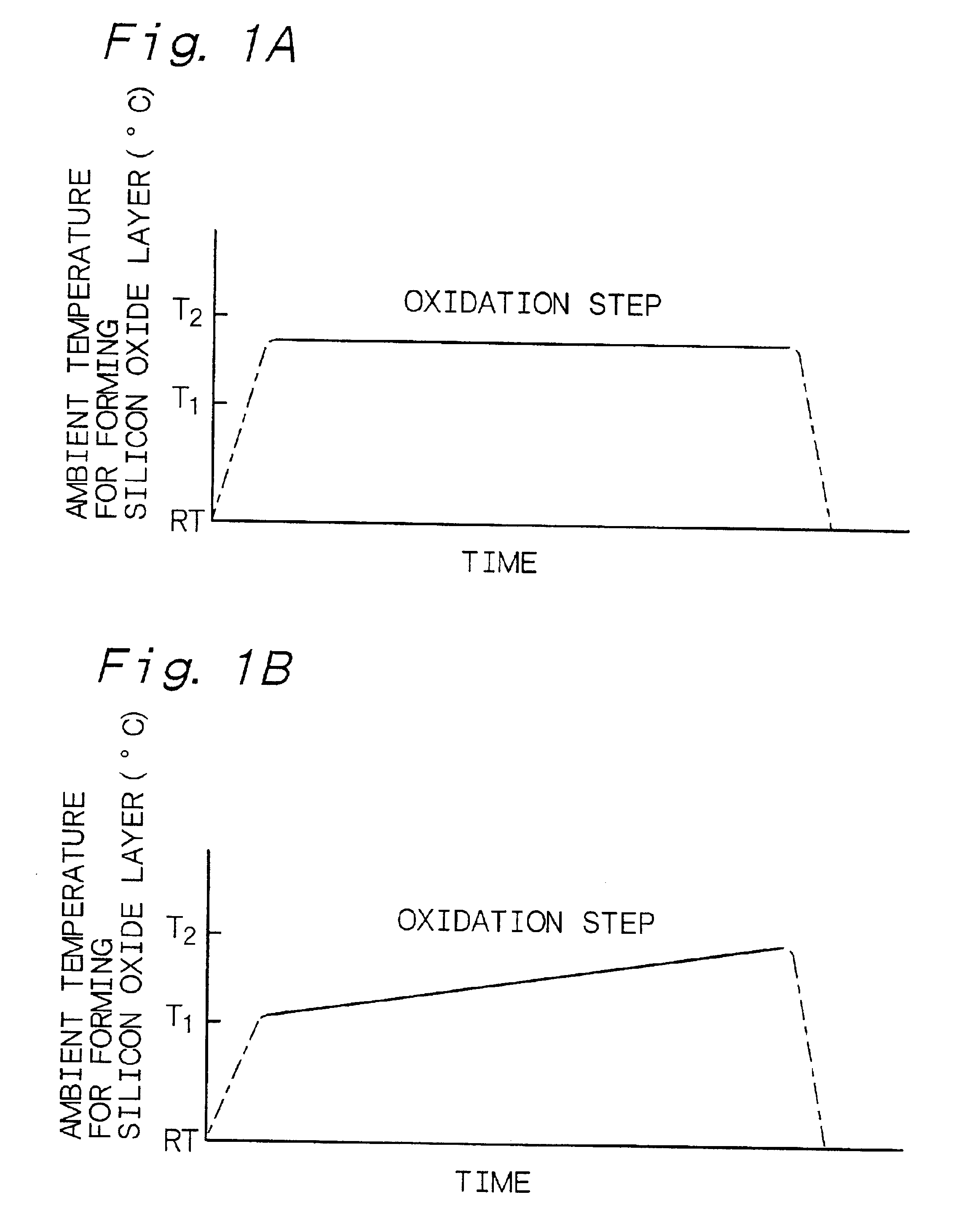
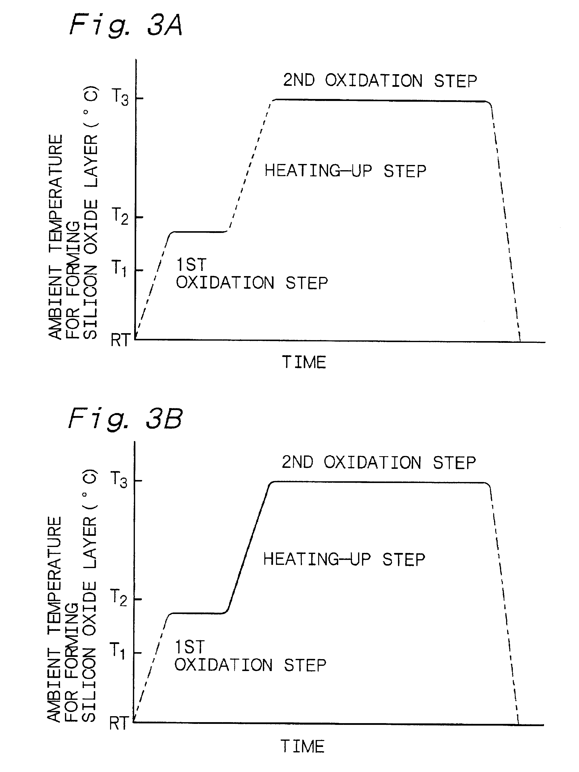
Example 1 is concerned with the preferred first embodiment A of the method of forming a silicon oxide layer according to the first aspect of the present invention, and is further concerned with the method of forming a silicon oxide layer according to the second aspect of the present invention. Example 1 uses a vertical-type processing apparatus having one process chamber for forming a silicon oxide layer, and a first oxidation step and a second oxidation step are carried out in the process chamber. Further, the first oxidation step and the second oxidation step are carried out with a batch processing. A heating-up step is included between the first oxidation step and the second oxidation step. Specifically, Example 1 used the vertical-type processing apparatus as shown in FIG. 13. A silicon semiconductor substrate was used as a silicon layer. A formed silicon oxide layer was to function as a gate oxide. Example 1 used an oxidation method using pyrogenic gas as an oxidation method us...
example 2
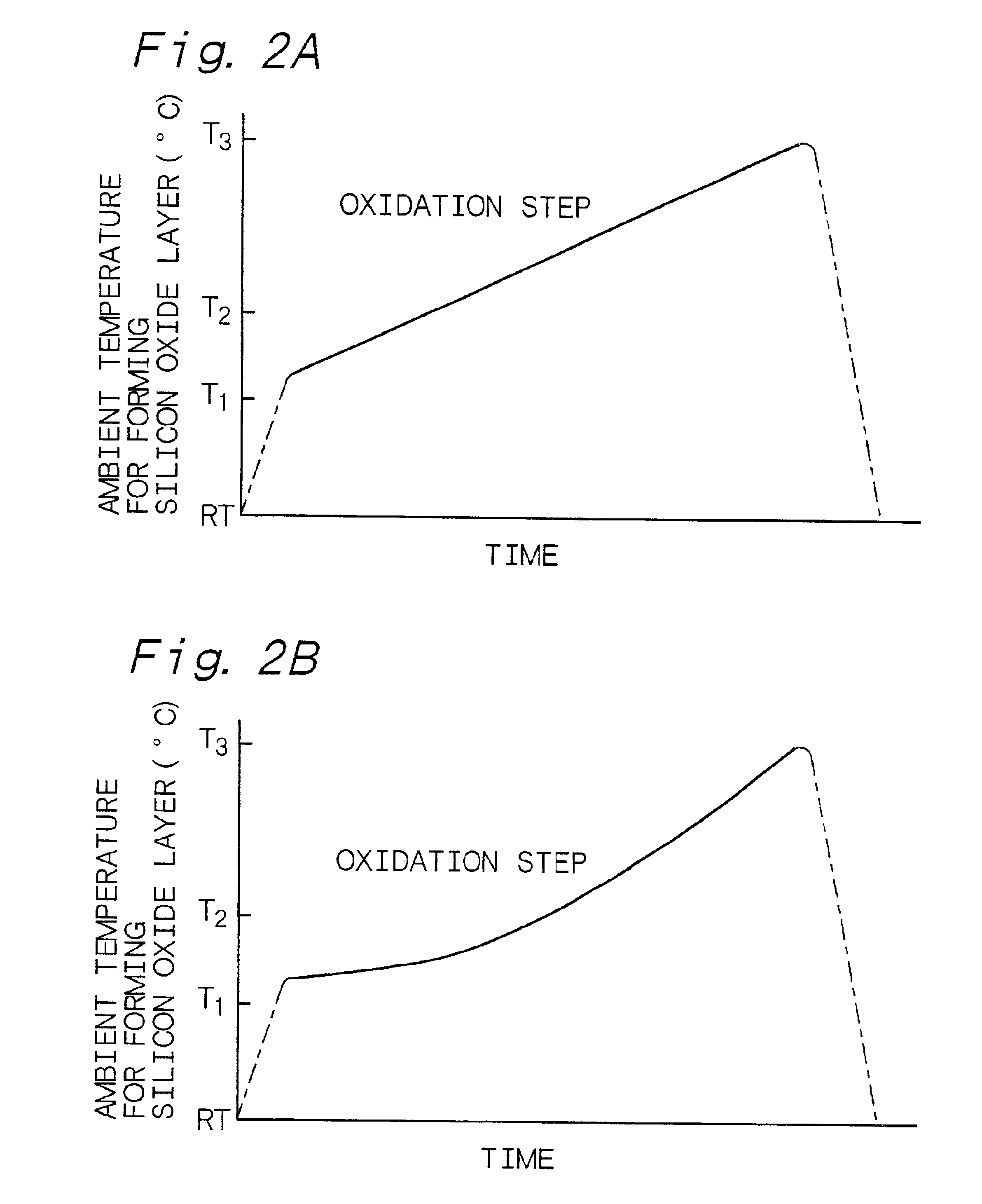
Example 2 is a variant of Example 1. In Example 2, the ambient temperature in the process chamber 10 was raised up to 800.degree. C. with the heater 14 through the liner tube 16 without terminating the introduction of the wet gas into the process chamber 10 in place of [Step-140] in Example 1. In Example 2, the formation of a silicon oxide layer was continued in the heating-up step as well. In the step corresponding to [Step-130] in Example 1, a silicon oxide layer having a thickness of 1.0 nm was formed. Any other procedures in Example 2 were the same as those in Example 1. FIG. 18 schematically shows an ambient temperature profile in Example 2.
example 3
Example 3 is also a variant of Example 1. In Example 3, an epitaxial silicon layer having a thickness of 10 .mu.m was formed on a silicon semiconductor substrate by a known method. A silicon oxide layer was formed on the surface of the epitaxial silicon layer, and further, MOS capacitors were formed, in the same manner as in [Step-110] to [Step-180] in Example 1. The silicon oxide layer had a total thickness of 4.0 nm. In the step equivalent to [Step-130], a silicon oxide layer having a thickness of 1.2 nm was formed.
PUM
| Property | Measurement | Unit |
|---|---|---|
| temperature | aaaaa | aaaaa |
| temperature | aaaaa | aaaaa |
| temperature | aaaaa | aaaaa |
Abstract
Description
Claims
Application Information