Single or multi-layer printed circuit board with recessed or extended breakaway tabs and method of manufacture thereof

a printed circuit board and multi-layer technology, applied in the direction of printed circuit aspects, printed circuit non-printed electric components association, transportation and packaging, etc., can solve the problems of increasing and reducing the number of printed circuit boards

Inactive Publication Date: 2005-01-18
PPG IND OHIO INC
View PDF15 Cites 28 Cited by
  • Summary
  • Abstract
  • Description
  • Claims
  • Application Information

AI Technical Summary

Benefits of technology

The method can also include providing a second conductive sheet and selectively removing one or more portions of the second conductive sheet to form a second panel having a second circuit board that is coupled to a disposable part of the second panel by at least one tab that extends from an edge of the second circuit board to an edge of the disposable part of the second panel. An insulating coating is applied to the second circuit

Problems solved by technology

The existing methods of cutting printed circuit boards from larger panels are unsatisfactory for high density boards because the limited dimensional stability of the printed circuit boards does not allow registration of one high density pattern to the next on the larger panel.
Cut lines made around the periphery of the printed circuit board further weaken the panel material, exasperating misregistration of one pattern to the next.
In high performance systems, however, as the

Method used


Image

  • Single or multi-layer printed circuit board with recessed or extended breakaway tabs and method of manufacture thereof
  • Single or multi-layer printed circuit board with recessed or extended breakaway tabs and method of manufacture thereof
  • Single or multi-layer printed circuit board with recessed or extended breakaway tabs and method of manufacture thereof

Examples


first embodiment

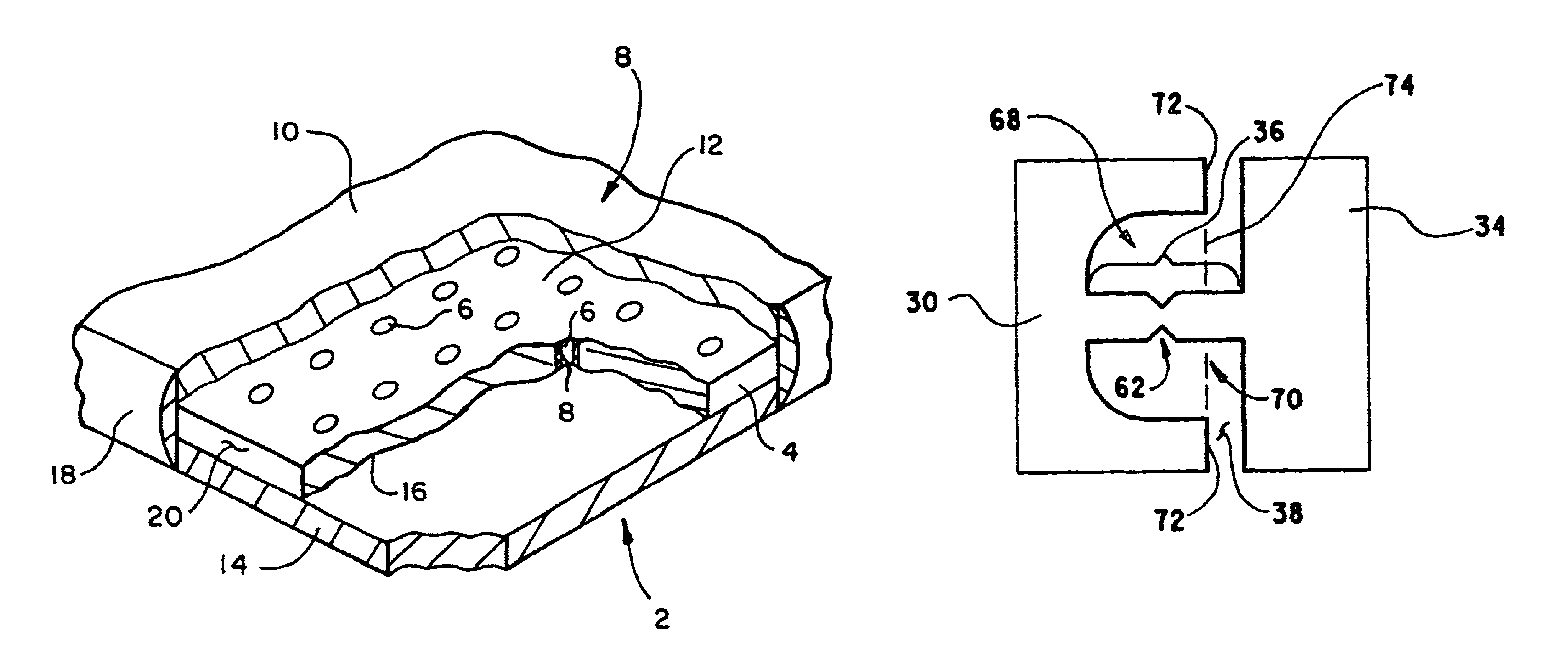
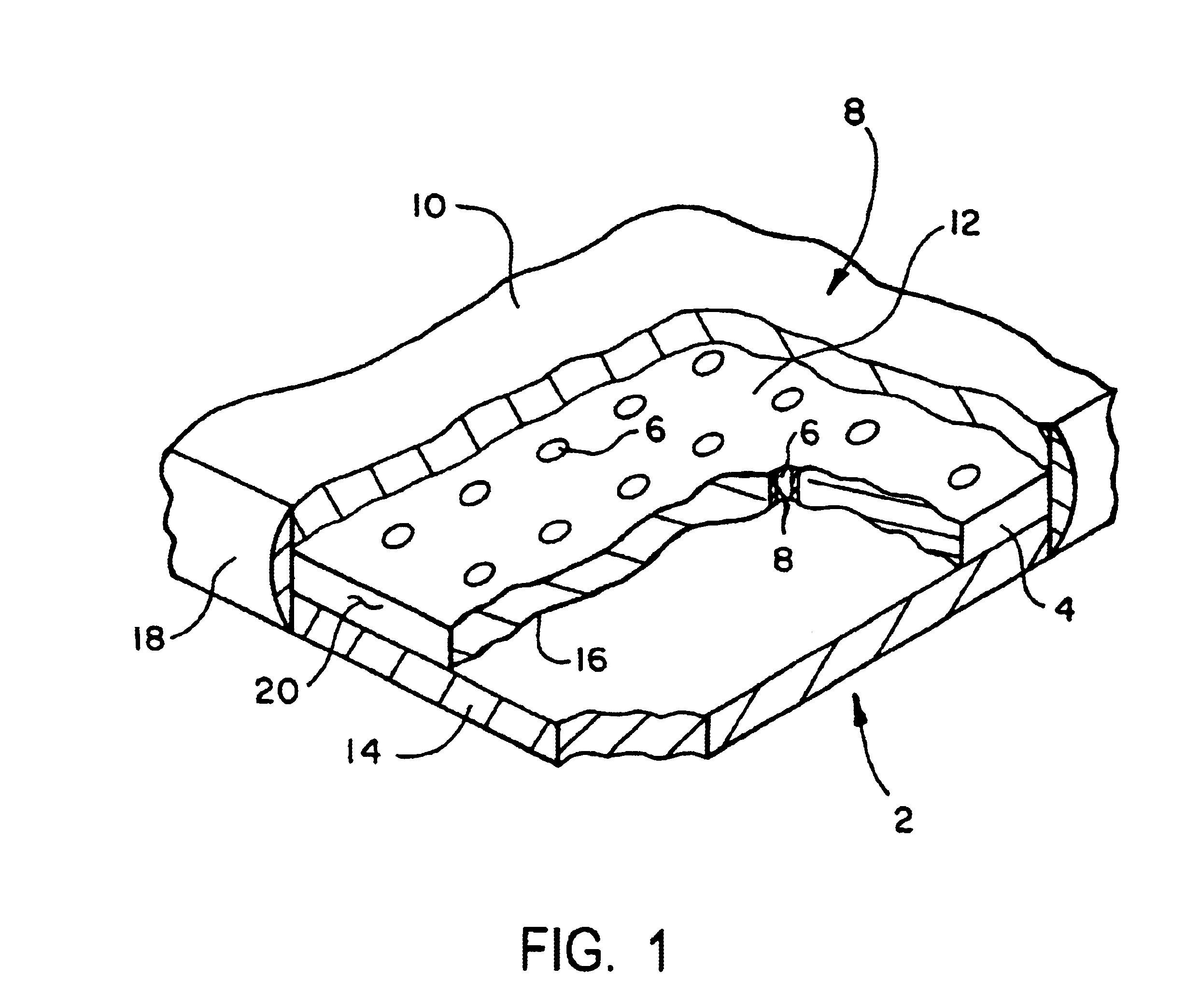
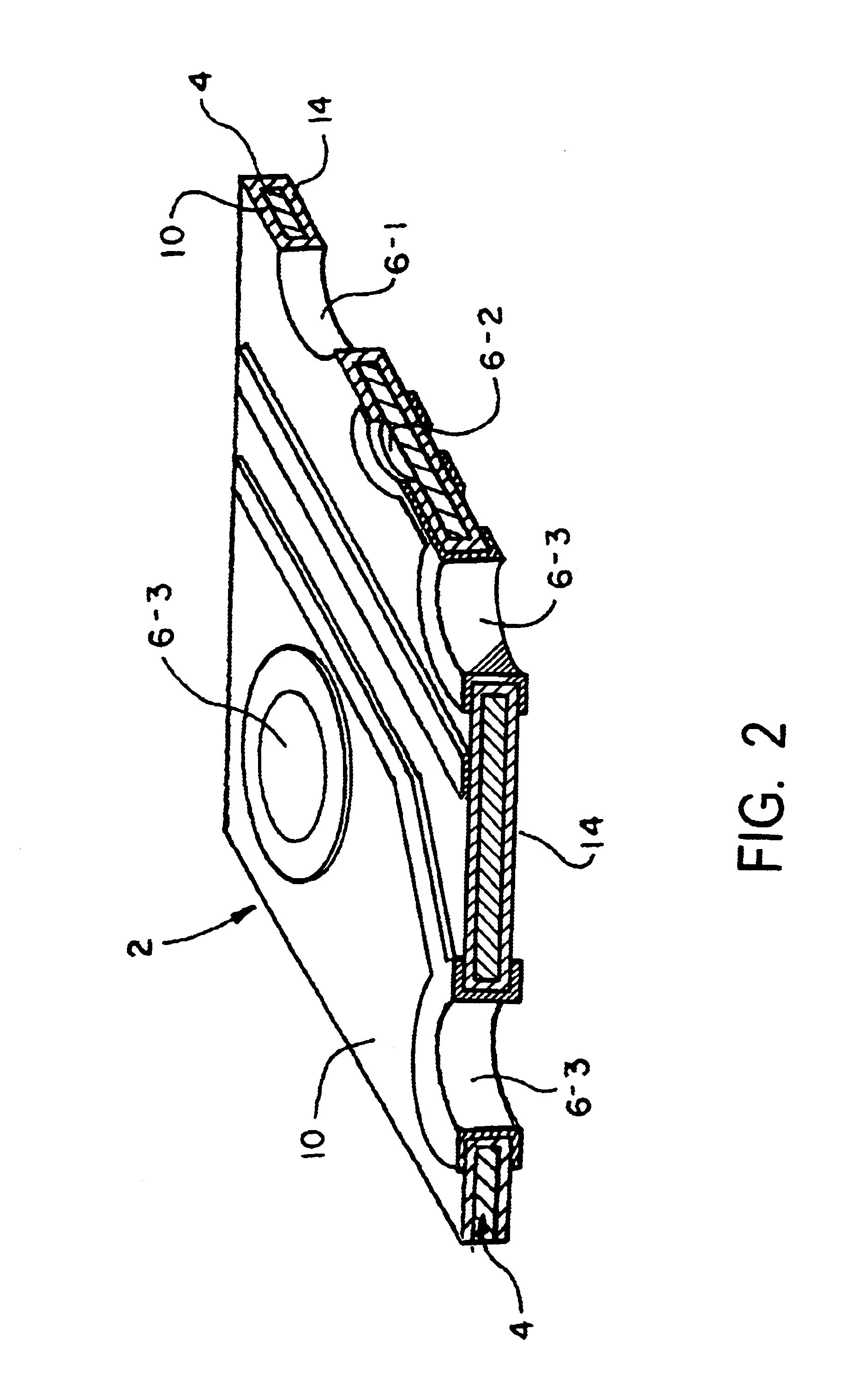
With reference to FIG. 3, in accordance with the invention, one or more first printed circuit board (PCB) layers 30 are fabricated as part of a panel 32. Each first PCB layer 30 is surrounded by a disposable part 34 of panel 32. In accordance with the present invention, each first PCB layer 30 is coupled to disposable part 34 of panel 32 by one or more tabs 36.

The general steps to prepare panel 32 to the form shown in FIG. 3 will now be described. Initially, a first conductive sheet, like conductive sheet 4, of the size of panel 32 is provided. This sheet can either be a solid sheet or a perforate sheet depending on the application. Next, cut lines or slots 38 are formed in the conductive sheet by pattern etching or a machine cutting or routing process to define the perimeter of each first PCB layer 30 of panel 32. These slots 38 are interrupted by tabs 36 which hold each first PCB layer 30 to disposable part 34 during processing.

Next, an electrically insulative coating, like coatin...

second embodiment

With reference to FIGS. 10 and 11, if desired, panel 98 can be laminated to a panel 106 in a manner known in the art with first PCB layer 90 in registry with a second PCB layer 102 of panel 106 to form a multi-layer PCB assembly 104, shown best in FIGS. 11-13. Second PCB layer 102 is part of panel 106 that includes tabs 108 and disposable part 110. One or more tabs 108 can each include a mounting hole 112 that can be utilized to couple tab 108 to appropriate mechanical hardware or electrical circuitry. In a manner similar to PCB layers 30 and 42 and tabs 36 and 48, respectively, second PCB layer 102 and tabs 108 can be formed from an electrically conductive sheet coated with an electrically insulative coating. However, in this second embodiment, the electrically insulative coating can be omitted from each tab 108 or can be removed from each tab 108 after deposit.

A circuit pattern 114 can be formed on one or both surfaces of second PCB layer 102 utilizing photolithographic processing...


PUM

PropertyMeasurementUnit
Electrical conductoraaaaaaaaaa
Perimeteraaaaaaaaaa

Abstract

A circuit board layer 2 in accordance with the present invention includes a conductive sheet 4 sandwiched between an insulating top layer 10 and an insulating bottom layer 14. The top and bottom layers 10 and 14 and the conductive sheet 4 define the circuit board layer 2 having an edge that includes an edge 20 of the conductive sheet 4. An insulating edge layer 18 covers substantially all of the edge 20 of the conductive sheet 4.

Description

BACKGROUND OF THE INVENTIONPresently, printed circuit boards are fabricated as part of a larger panel. Each printed circuit board can be configured in any shape, although most printed circuit boards in common use are made in rectangular shapes of standard sizes. When fabrication of a printed circuit board is complete, it is cut and separated from the larger panel, mostly by way of a machine cutting or routing process in which a channel is cut around the printed circuit board. In certain designs, the channel around the printed circuit board does not completely encircle the perimeter of the printed circuit board. Rather, tabs are left at several places around the perimeter of the printed circuit board to attach it to the larger panel until the board is singulated from the larger panel by breaking the tabs. Typically, metal planes in the printed circuit board do not extend to its edge where they would be cut by the routing process. In this way, no conductive metal is left exposed on th...

Claims


Application Information

Patent Timeline
IPC IPC(8): H05K3/00H05K3/46H05K3/44H05K1/05H05K3/06
CPCH05K3/0052H05K3/44H05K3/4641H05K3/002H05K1/056Y10T29/49167H05K3/4644H05K2201/0166H05K2201/0909H05K2201/0919H05K2201/09554H05K2203/135Y10T428/24322Y10T428/12361Y10T29/49156Y10T29/49126H01L2224/16225H01L2924/15174H05K3/00H05K3/06
Inventor WANG, ALAN E.OLSON, KEVIN C.DI STEFANO, THOMAS H.
Owner PPG IND OHIO INC
Why Eureka
Try Eureka