

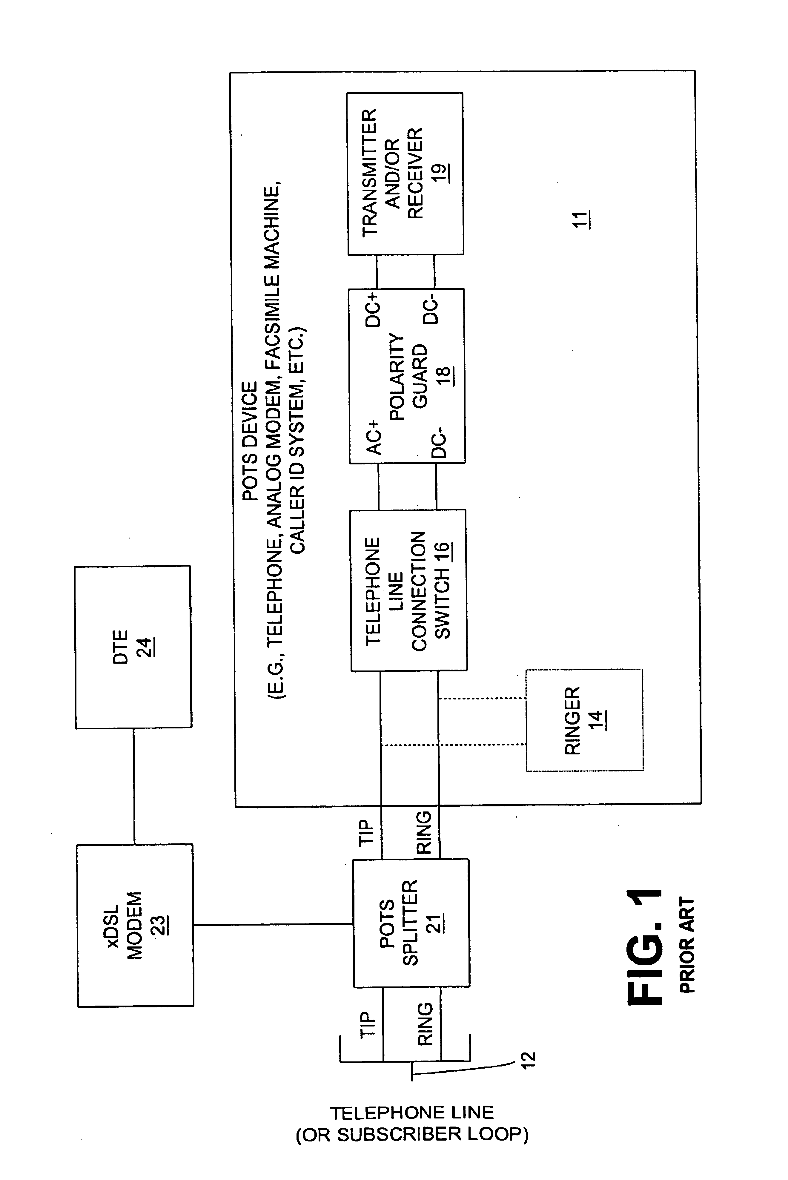
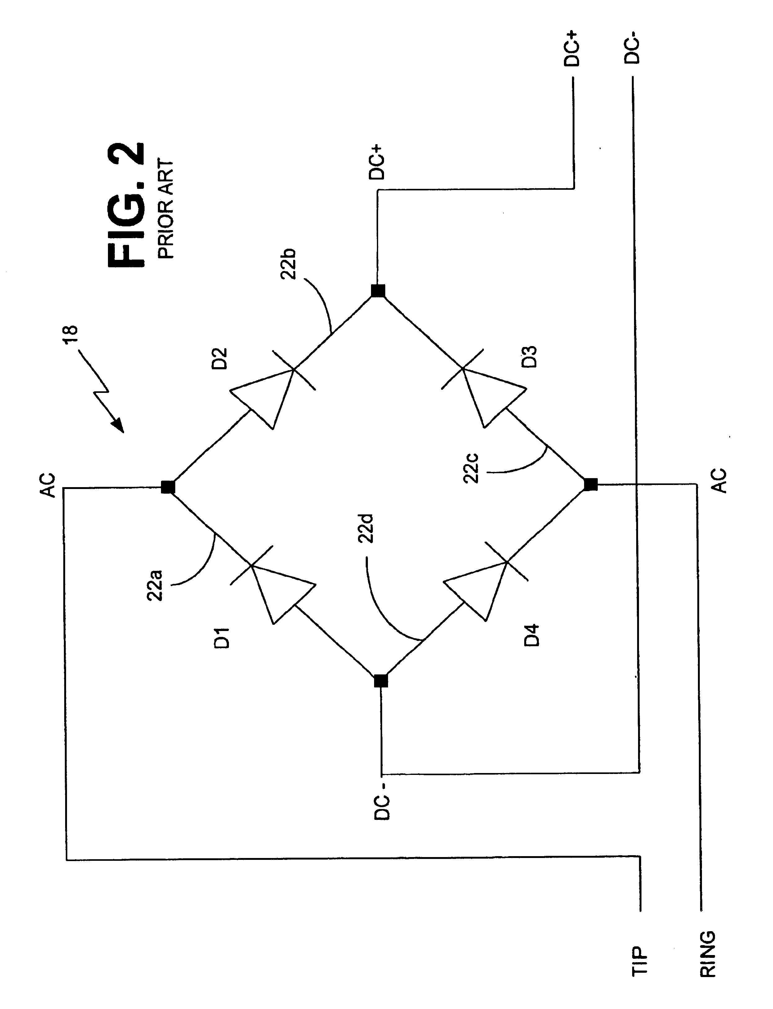
Linear polarity guard and method for DSL-ready pots devices
a linear polarity guard and pots technology, applied in the field of data communication and telephony, can solve the problems of expensive devices, undesirable installation time, labor and expense, and interference of dsl signal imd with dsl modem operation, and achieve the effect of reliable and efficient decoupling of pots channels and reducing interferen
- Summary
- Abstract
- Description
- Claims
- Application Information
AI Technical Summary
Benefits of technology
Problems solved by technology
Method used
Image

Examples
first embodiment
[0041]FIG. 5 is a circuit diagram of a first embodiment of the linear polarity guard 30 (FIG. 4) and is generally denoted by reference numeral 30′. This is currently the best mode known to the inventors for practicing the present invention. The linear polarity guard 30′ will exhibit the linear VI transfer function indicated by line 25′ in FIG. 3. The solid part of line 25′ indicates the usual linear operating region of the polarity guard 30′. (The small-dash part extending to the graph origin indicates the linear region that typically is not useable by the polarity guard 30′ because the enhancement mode MOSFETs are not sufficiently biased into the ohmic region for linear operation. However, MOSFETs can be fabricated with very low VON, therefore this unusable region near the graph origin can be minimized, if necessary.) The line 25′ graphically indicates the substantially linear relationship between input current and voltage drop (as well as output voltage) across the linear polarity...
second embodiment
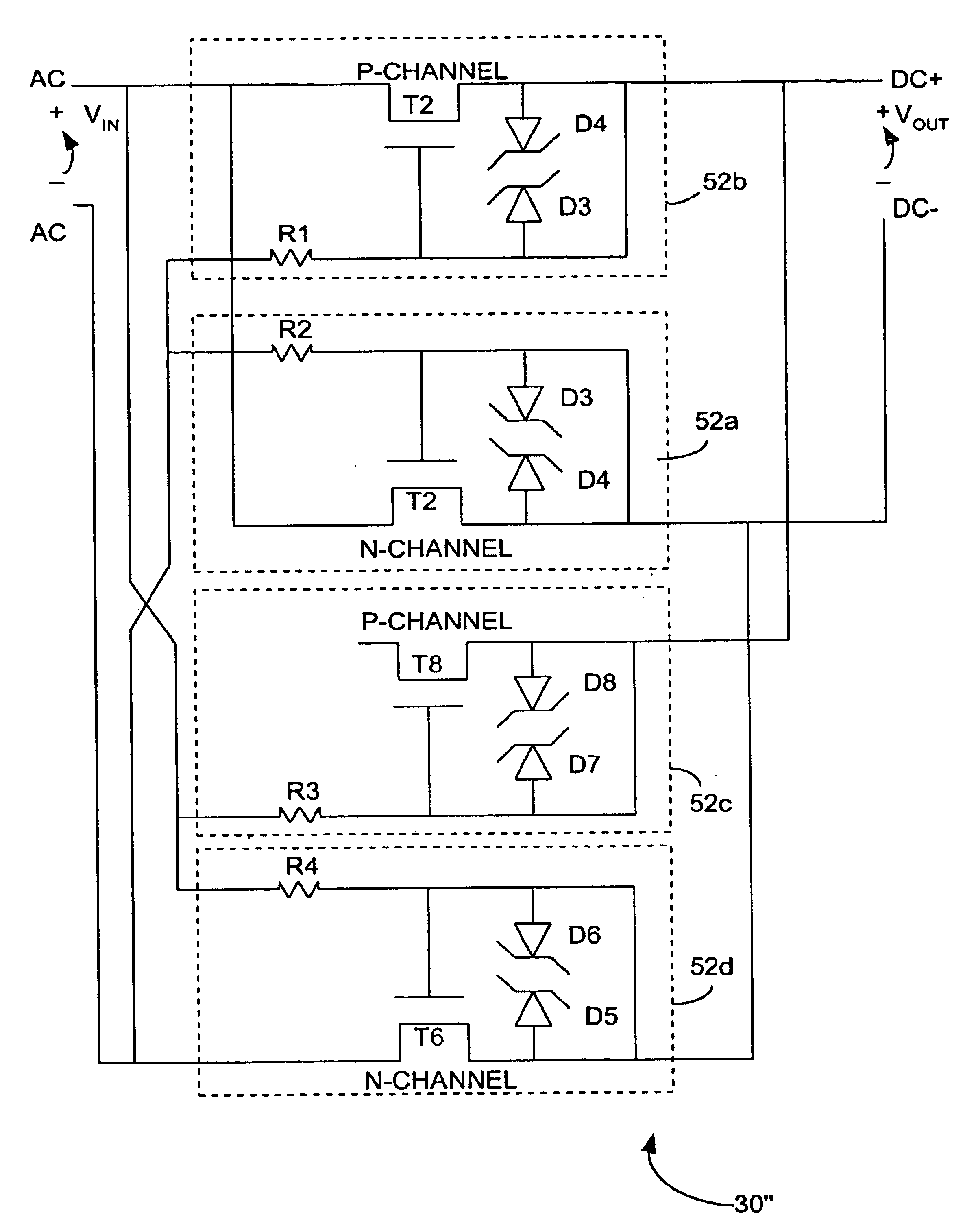
[0054]The configuration of the first embodiment can be simplified by eliminating the second series transistors T1, T3, T7, T5 along with their respective vestigial body diodes D10, D14, D11, D15, if the vestigial body diodes D9, D13, D12, D16 associated with corresponding transistors T2, T4, T8, T6 are eliminated or significantly minimized. This is the essence of the second embodiment of the linear polarity guard 30, which is shown in FIG. 6 and generally denoted by reference numeral 30″. At the present time, it is possible but difficult to fabricate such MOSFETs with specifications practical for POTS devices; however, it is envisioned that such MOSFETs will be more widely available in the future with the further advancement of fabrication techniques, and when this occurs, the second embodiment will likely be more desirable than the first, in light of its more simplified circuit design.
[0055]When FIG. 6 is built with transistors of the same channel-resistance as those transistors in...
PUM
 Abstract
Description
Claims
Application Information