Method for forming a self-aligned LTPS TFT

a thin film transistor and self-aligning technology, applied in the direction of transistors, electrical devices, semiconductor devices, etc., can solve the problems of high quality and low price of flat panels, misalignment or overlap, etc., and achieve the effect of avoiding the error resulting from the photo process

Inactive Publication Date: 2005-01-25
AU OPTRONICS CORP
View PDF3 Cites 14 Cited by
  • Summary
  • Abstract
  • Description
  • Claims
  • Application Information

AI Technical Summary

Benefits of technology

It is therefore one object of the present invention to provide a method for forming an LTPS TFT that can self align the lightly

Problems solved by technology

As the requirements of high quality displays increase, flat panels with high quality and low price are demanding in the future.
However, when defining the pattern of the photo resist mask in a photo process by a stepper or a scanner, misalignment or o

Method used


Image

  • Method for forming a self-aligned LTPS TFT
  • Method for forming a self-aligned LTPS TFT
  • Method for forming a self-aligned LTPS TFT

Examples


Embodiment Construction

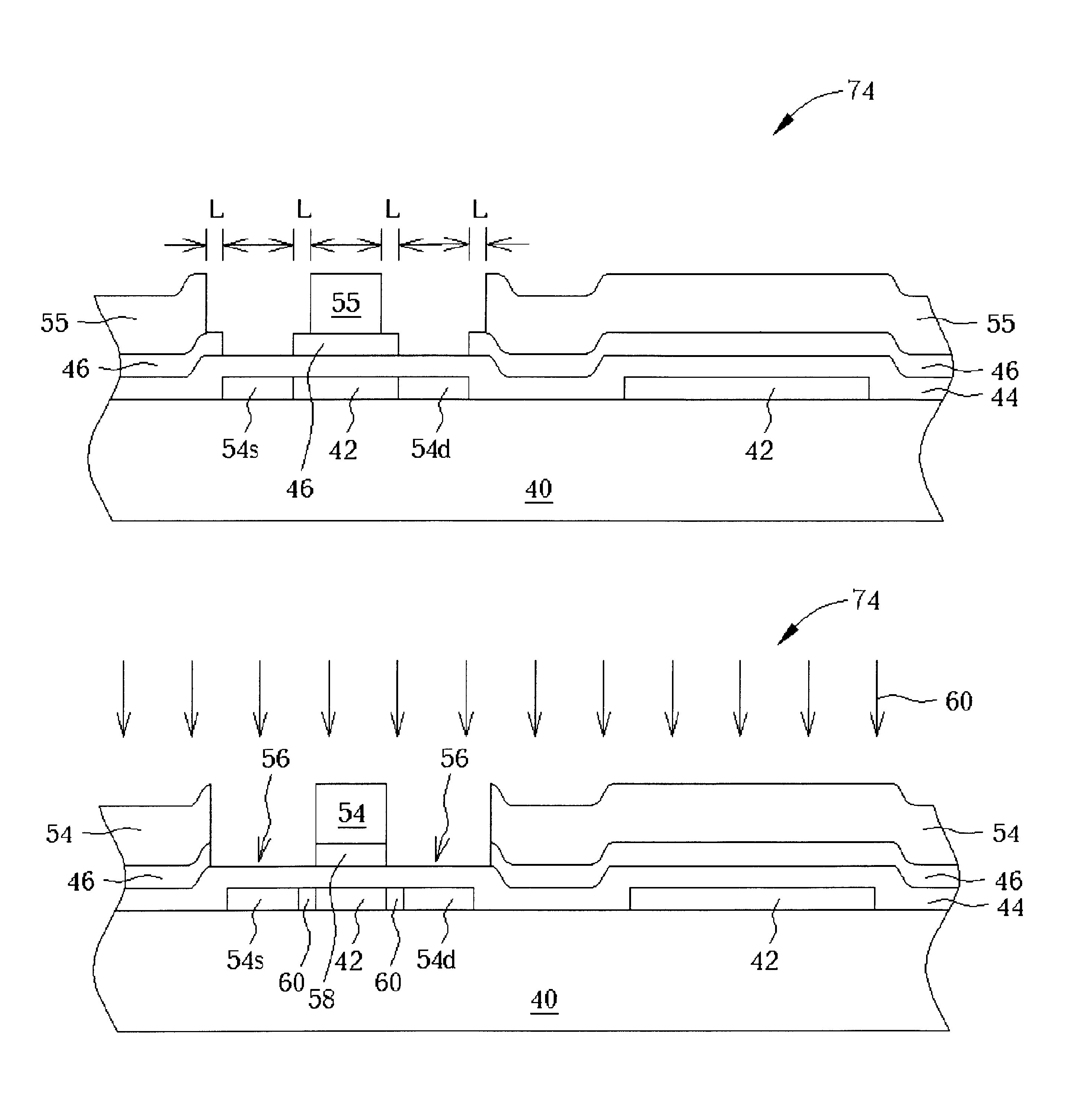
The present invention provides a method for simultaneously forming an NLTPS TFT and a PLTPS TFT. However, the application of the present invention is not limited by the embodiments. In a preferred embodiment of the present invention, the method of the present invention can be also applied to form an LTPS CMOS TFT composed of an NLTPS TFT and a PLTPS TFT. The LTPS CMOS TFT, NLTPS TFT, or PLTPS TFT of the present invention is formed in a periphery circuit area of an LCD for being a logic device. Moreover, the NLTPS TFT used to be a switching device could also be formed by the method of the present invention in a pixel array area of the LCD.

An example of forming an LTPS CMOS TFT 74 is used here for illustrating the method of the present invention. FIGS. 6-14 are schematic diagrams of a method for forming the LTPS CMOS TFT 74 according to a preferred embodiment of the present invention. As shown in FIG. 6, the LTPS CMOS TFT 74 is formed on a substrate 40, and the substrate 40 surface co...


PUM


Abstract

A method for forming a self-aligned low temperature polysilicon thin film transistor (LTPS TFT). First, active layers of a N type LTPS TFT (NLTPS TFT) and a P type LTPS TFT (PLTPS TFT) are formed on a substrate, and a gate insulating (GI) layer is formed on the substrate. Then, a source electrode, a drain electrode, and lightly doped drains (LDD) of the NLTPS TFT are formed. Further, gate electrodes of the NLTPS TFT and the PLTPS TFT are formed on the gate insulating layer. Finally, the gate electrode of the PLTPS TFT is utilized to form a source electrode and a drain electrode in the active layer of the PLTPS TFT.

Description

BACKGROUND OF INVENTION1. Field of the InventionThe present invention relates to a method for forming a low temperature polysilicon thin film transistor (LTPS TFT), and more particularly, to a method for forming a self-aligned LTPS TFT.2. Description of the Prior ArtA liquid crystal display is broadly applied to portable electronic apparatuses, such as notebooks and personal digital assistants (PDAs), because of its thin display panel, low power consumption, and low-radiation. As the requirements of high quality displays increase, flat panels with high quality and low price are demanding in the future. An LTPS TFT, which is an actively driving TFT, is one of the important technologies for achieving the goal.An LTPS TFT-LCD includes at least a transparent substrate, a pixel array region, a scan line driving circuit region, and a data line driving circuit region. The pixel array region comprises a plurality of parallel scan lines, a plurality of parallel data lines, and a liquid cryst...

Claims


Application Information

Patent Timeline
IPC IPC(8): H01L21/02H01L29/786H01L29/66H01L21/70H01L21/336H01L27/12H01L21/84H01L21/77
CPCH01L27/1214H01L29/78675H01L29/78621H01L29/66757H01L27/1288
Inventor CHANG, CHIH-CHIN
Owner AU OPTRONICS CORP
Why Eureka
Try Eureka