Semiconductor image position sensitive device

Inactive Publication Date: 2005-01-25
RIKEN
View PDF9 Cites 2 Cited by
  • Summary
  • Abstract
  • Description
  • Claims
  • Application Information

AI Technical Summary

Benefits of technology

The present invention has been made in view of the above described problems involved in the prior art. An object of the invention is to provide a semicondu

Problems solved by technology

However, it is not so easy that the resistance layer Rp being a dividing resistance for calculating an image position is formed stably as a uniform thin film having a predetermined resistivity, and as a result, such resistivity cannot be made constant, whereby a distribution of the resistivity becomes scattered.
Thus, there is a problem that the scattering becomes a factor of an error in sensing for image position.
For this reason, it has been pointed out that there is such a problem that when a noise light such as background light occupying a large area though brightness is not high exists in a wide region in a peripheral section of an objective spot image, a significant error

Method used


Image

  • Semiconductor image position sensitive device
  • Semiconductor image position sensitive device
  • Semiconductor image position sensitive device

Examples


Embodiment Construction

Examples of preferred embodiments of the semiconductor image position sensitive device according to the present invention will be described in detail hereinafter in conjunction with the accompanying drawings.

It is to be noted that the same or equivalent components as or to those of FIGS. 1 through 4 are designated by the same reference characters in FIGS. 5 through 9 wherein the detailed description relating thereto will be omitted.

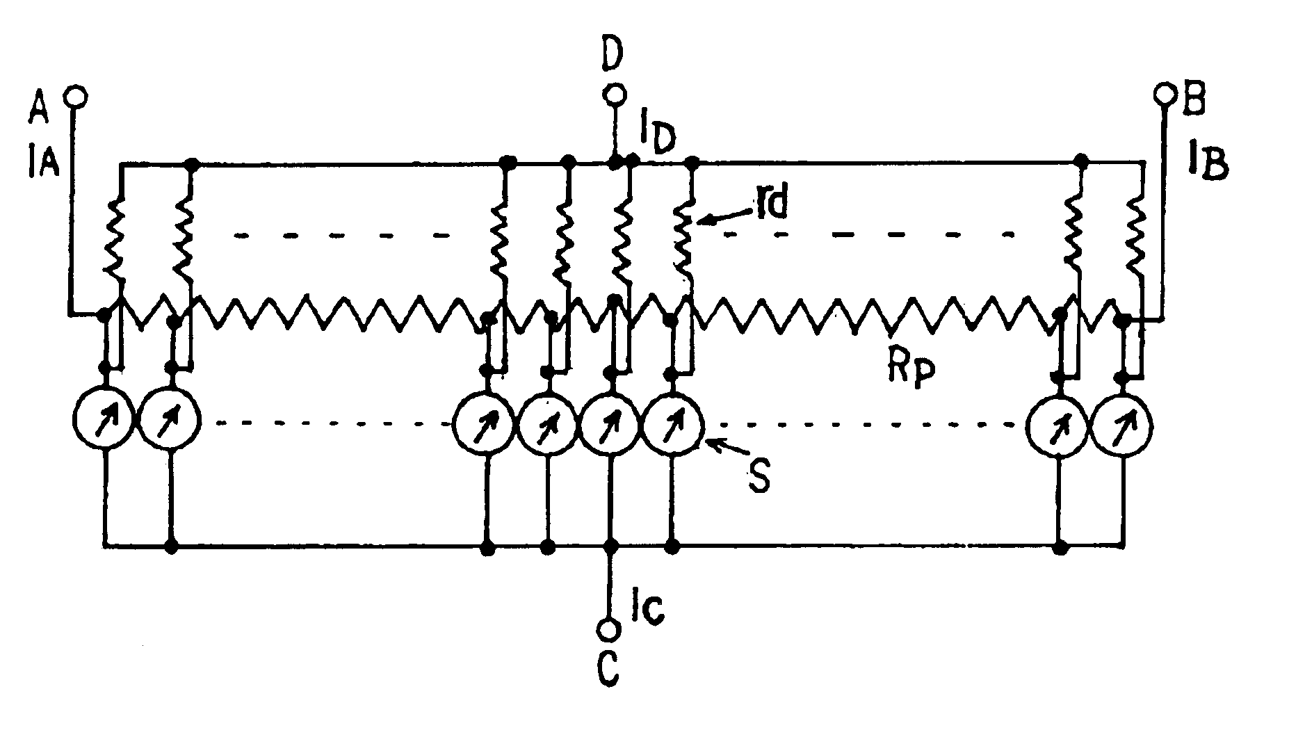
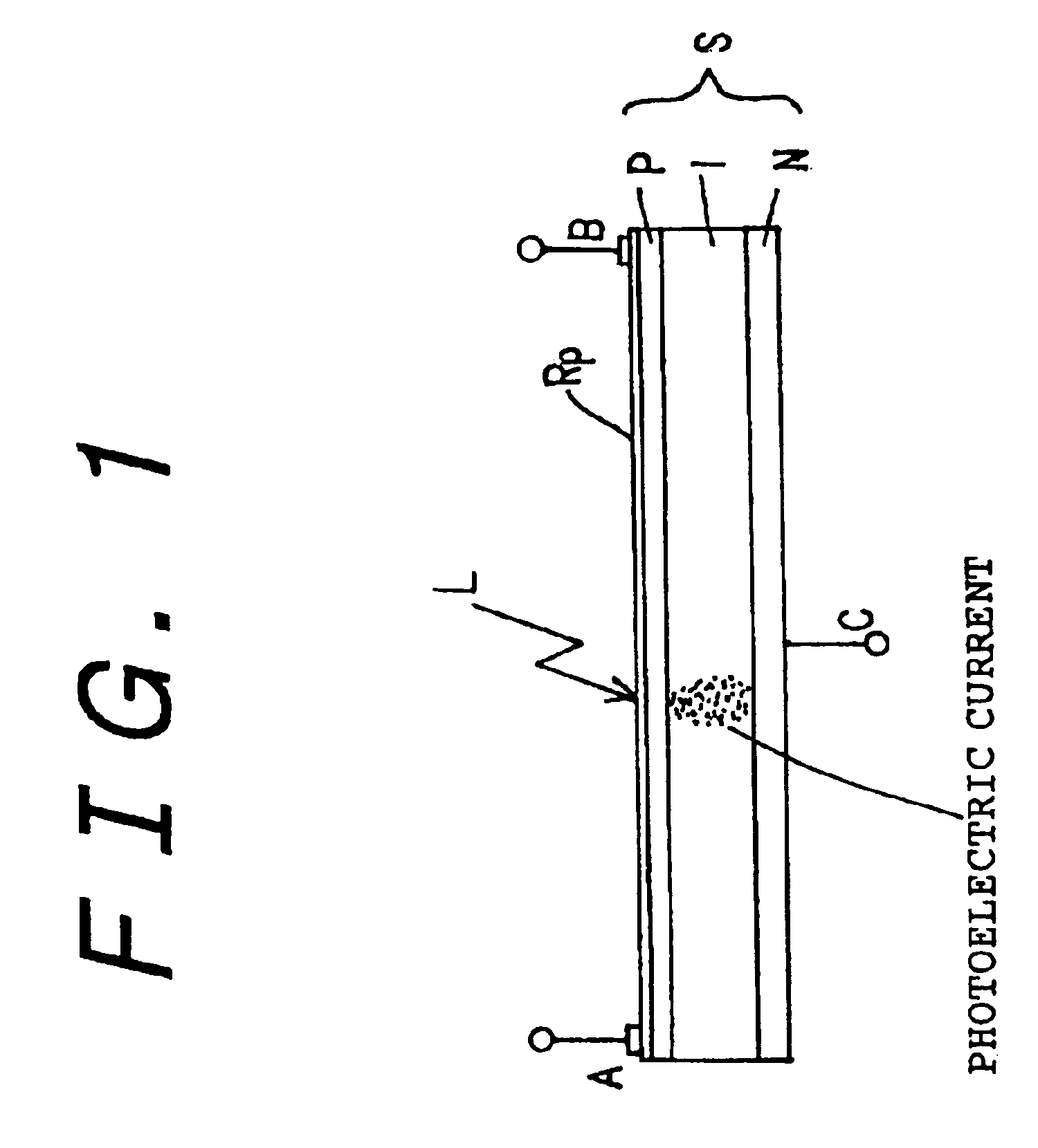
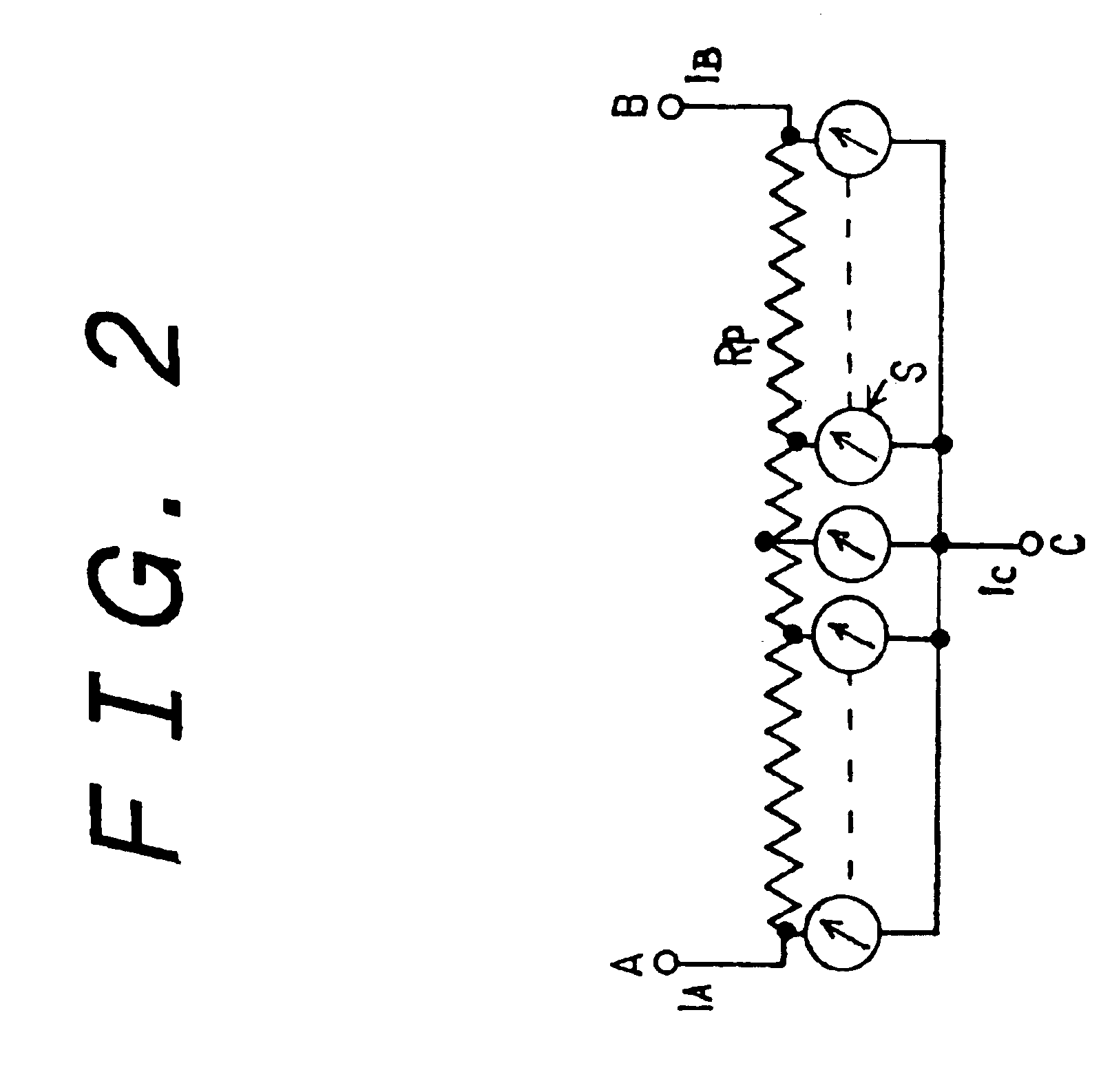
FIG. 5 shows an example of preferred embodiments of a semiconductor image position sensitive device according to the present invention wherein the semiconductor image position sensitive device is constituted in such that an electric current obtained by subtracting-an amount of electric current corresponding to a current density of noise light such as background light from the photoelectric current shown in FIG. 4(b) flows into a dividing resistance for calculating an image position.

More specifically, FIG. 5 shows an equivalent circuit representing an exam...


PUM


Abstract

In order to reduce errors in sensing an image position derived from noise light such as background noise, a semiconductor image position sensing device is provided with a photoelectric layer generating a photoelectric current in a portion onto which light was input in response to intensity of the light input to the photoelectric layer, a resistance layer laminated on the photoelectric layer in which the photoelectric current generated in the photoelectric layer flows into a portion corresponding to that onto which the light was input, and signal current output terminals wherein the photoelectric current generated in the photoelectric layer is distributed in a ratio in response to a resistance value between the signal current output terminals and the resistance layer defined at a position where the photoelectric current flowed into the resistance layer and from which the photoelectric current is output as an electric current obtained by summing currents over the whole sensing sections altogether, comprising further a resistance subtracting a photoelectric current having a predetermined distribution of electric current density from photoelectric currents generated in respective portions of the photoelectric layer over the whole sensing sections, and the photoelectric current subtracted by means of the resistance being adapted to flow into the resistance layer.

Description

BACKGROUND OF THE INVENTION1. Field of the InventionThe present invention relates to a semiconductor image position sensing device, and more particularly to a semiconductor image position sensing device for sensing a position of a spot image at high speed. Especially, the invention relates to a semiconductor image position sensing device used in a sensor for determining an optical position in a variety of automation systems or a variety of optical measuring systems and suitable for realizing a high-speed and simple sensing system or measuring system.2. Description of the Related ArtHeretofore, a semiconductor image position sensitive device has been known as a sensor for detecting simply a spot image position at high speed.In general, a semiconductor image position sensitive device is composed of a photoelectric layer, a dividing resistance layer laminated on the photoelectric layer, and signal current output terminals connected to the dividing resistance layer. Such a semiconductor...

Claims


Application Information

Patent Timeline
IPC IPC(8): H01L31/02G01B11/00G01C3/06H01L21/66
CPCH01L31/02024H01L22/00
Inventor IDESAWA, MASANORIFUJITA, TOYOMIYANO, YASUSHIGE
Owner RIKEN
Why Eureka
Try Eureka