Five transistor CMOS pixel

Inactive Publication Date: 2005-01-25
TELEDYNE DIGITAL IMAGING INC
View PDF13 Cites 42 Cited by
  • Summary
  • Abstract
  • Description
  • Claims
  • Application Information

AI Technical Summary

Benefits of technology

It is an object to the present invention to achieve a fully integrated (no external shutter) and electronically adjustable sensor. This is achieved by adding one transistor to a known 4T pixel and controlling the clocking voltages as described herein. It is

Problems solved by technology

The Tsang, et al. pixel does not allow for electronically “shuttered” image acquisition.
This pixel does not provide protection against a rolling shutter artifact (as described herein) at the same time as antiblooming and exposure control.
However, the pixel does not provided antiblooming functionality at the same time as it provides protection against the rolling shutter artifact.
However, the pixel does not pr

Method used


Image

  • Five transistor CMOS pixel
  • Five transistor CMOS pixel
  • Five transistor CMOS pixel

Examples


Embodiment Construction

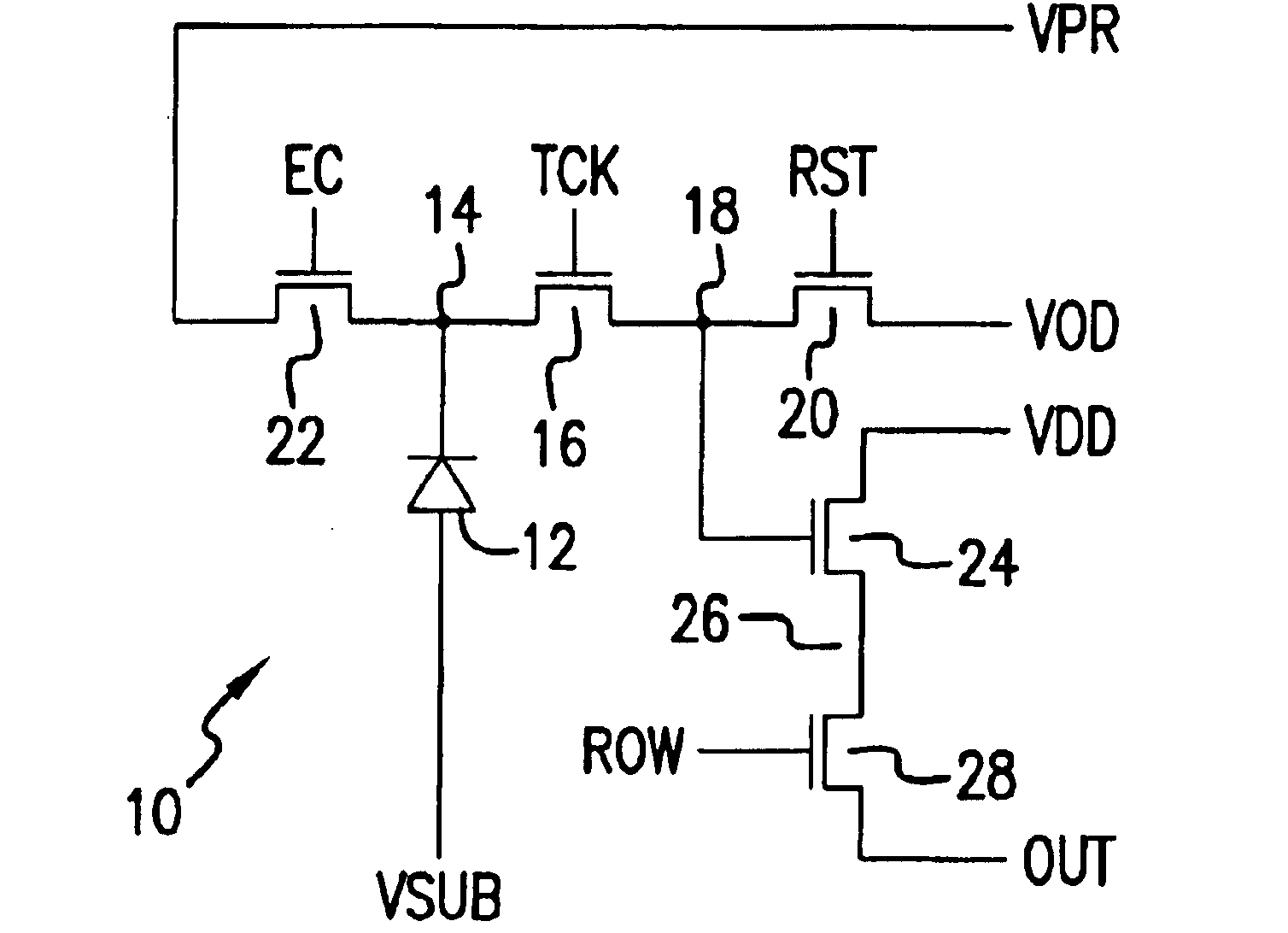
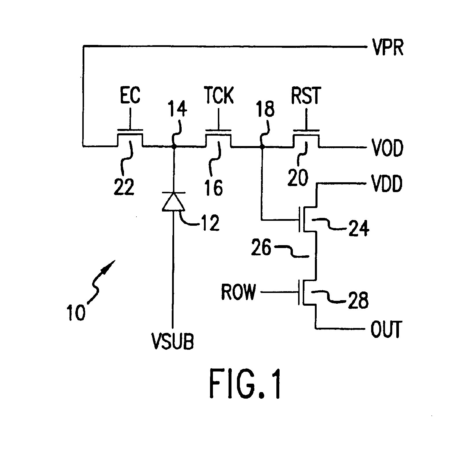
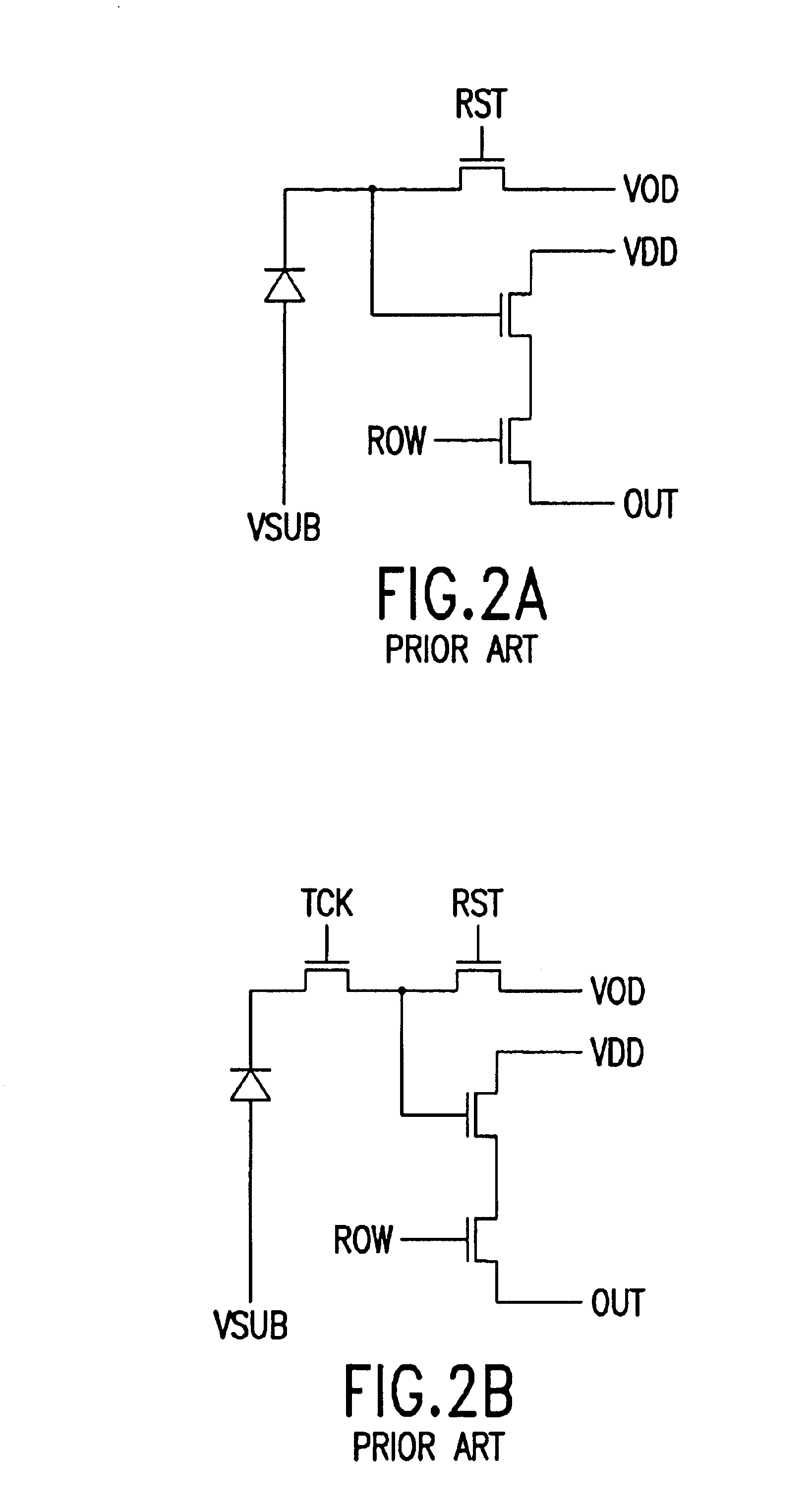
In FIG. 1, a new pixel includes a light shield (not shown in FIG. 1 for clarity) overtop of a sense node (i.e., junction 18) and exposure control gate transistor 22 off of the photosite. The sense node (junction 18) includes the diode region between reset gate transistor 20 and transfer gate transistor 16. However, the light shield (not shown in the circuit schematic for clarity) prevents generation of photo charge in the sense node. Advantages of this pixel are that the pixel can be implemented in such a way that the “rolling shutter” problem associated with conventional CMOS image sensors can be eliminated while at the same time allowing for antiblooming (AB) operation and electrode exposure control (EC) operation. The new pixel is a 5-transistor architecture (“5T”). In contrast, a “4T” pixel can be operated to either eliminate rolling shutter problem or allow for AB / EC functionality, but not both at the same time.

Another feature of the 5T pixel is the specific timing and biasing ...


PUM


Abstract

A method of sensing radiation in a pixel includes applying a transfer clock signal, applying a pixel reset clock signal, and applying a pixel reset voltage. The applying a transfer clock signal applies the transfer clock signal to a gate electrode of a transfer gate transistor. The applying a pixel reset clock signal applies the pixel reset clock signal to a gate electrode of the pixel reset transistor. The applying a pixel reset voltage applies the pixel reset voltage to a drain of the pixel reset transistor. The method further includes switching the transfer clock signal to a high state, switching the pixel reset clock signal to a high state, switching the pixel reset voltage to a low state, switching the pixel reset voltage to a high state, and switching the pixel reset clock signal to a low state at a beginning of an integration cycle.

Description

BACKGROUND OF THE INVENTION1. Field of the InventionThe present invention relates to a novel pixel architecture for high speed motion capture CMOS image sensors.2. Description of Related ArtFIGS. 2A and 2B are circuit schematics of conventional CMOS pixels known as a 3T pixel (for three transistor pixel) and a 4T pixel (for four transistor pixel). The 3T pixel has a reverse biased photodiode coupled between substrate voltage VSUB and the reset gate transistor. When operated, an RST signal applied to the electrode of the reset gate transistor causes a reverse bias to be set on the photodiode equal to output drain voltage VOD less VSUB. Between drain supply VDD and output signal terminal OUT is coupled two series transistors. The drain of a first transistor is coupled directly to VOD, and a gate of the first transistor is coupled to the cathode of the photodiode so that the first transistor operates as a source follower. The source of the source follower transistor is coupled through ...

Claims


Application Information

Patent Timeline
IPC IPC(8): H01L29/04H01L29/02H01L31/06H01L31/062
CPCH04N5/3745H04N5/3594H04N25/623H04N25/77
Inventor FOX, ERIC CHARLES
Owner TELEDYNE DIGITAL IMAGING INC
Why Eureka
Try Eureka