Probe pin assembly

a technology of probe pins and assemblies, applied in the direction of individual semiconductor device testing, semiconductor/solid-state device testing/measurement, instruments, etc., can solve the problems of difficult to provide a probe pin with an appropriate spring constant, the required pin pitch of the probe pin used in ic testing has become very small, and the circuit pattern has become extremely fine. to prevent contact error

Inactive Publication Date: 2005-01-25
KIMOTO GUNSEI
View PDF8 Cites 68 Cited by
  • Summary
  • Abstract
  • Description
  • Claims
  • Application Information

AI Technical Summary

Benefits of technology

Thanks to the above structure, since the deformation units of the lateral parallel pin array and those of the vertical parallel pin array are arranged at different heights, the perpendicular-type probe pins of the lateral parallel pin array do not interfere with those of the vertical parallel pin array on the same plane over the chip under test. Thus the probe pins for each chip under test can be accommodated in the space just above each chip so that they do not extend to the adjacent space above another chip, thereby making multi-die contact or batch-die contact possible. Moreover, since each probe pin has a sufficient space above the chip under test for deformation, it becomes possible to prevent the contact error and positioning error during contact of the pin from exceeding tolerance.
According to the present invention, since the vertical-type probe pins occupy only the space above each chip under test and they do not extend to the adjacent space above another chip, thereby making multi-die contact or batch-die contact possible. Moreover, since each vertical-type probe pin has a sufficient space above the chip under test for deformation, it becomes possible to prevent the contact error and positioning error during contact of the pin from exceeding tolerance.
It is, therefore, an object of the present invention to provide a probe pin assembly that limits the space occupied by the probe pins for each chip under test to the space just above each chip so as not to extend to the adjacent space above another chip, when measuring the electric properties of a chip by establishing electric continuity by contacting probe pins to the electrode pads of the chip. Then multi-die contact or batch-die contact becomes possible to do.
Another object of the present invention is to provide a probe pin assembly that provides a sufficient space above the chip under test for the deformation of each probe pin and thereby prevent the contact error and positioning error during contact of the pin from exceeding tolerance.

Problems solved by technology

The prior art probe pin assembly, however, has a problem that the probe pins do not reach all the electrode pads of the LSI chips together when a number of chips are arranged close to each other on a wafer as is the case where a plurality of LSI chips are arranged in a grid pattern on the wafer.
Moreover, as the IC manufacturing technology is improved these years, the circuit pattern has become extremely fine and the required pin pitch of probe pins used in IC testing has also become very small.
Then it becomes difficult to provide a probe pin having an appropriate spring constant because the probe pin is not allowed to have a sufficient space needed for the installation of its deformation unit.
If the elastic deformation of a probe pin and its movable margin become small, an appropriate contact pressure is not provided between the probe pin and the electrode pad when there is, for example, a pin manufacturing error or a mechanical pin positioning error during contact.

Method used


Image

  • Probe pin assembly
  • Probe pin assembly
  • Probe pin assembly

Examples


embodiment 1

(Embodiment 1)

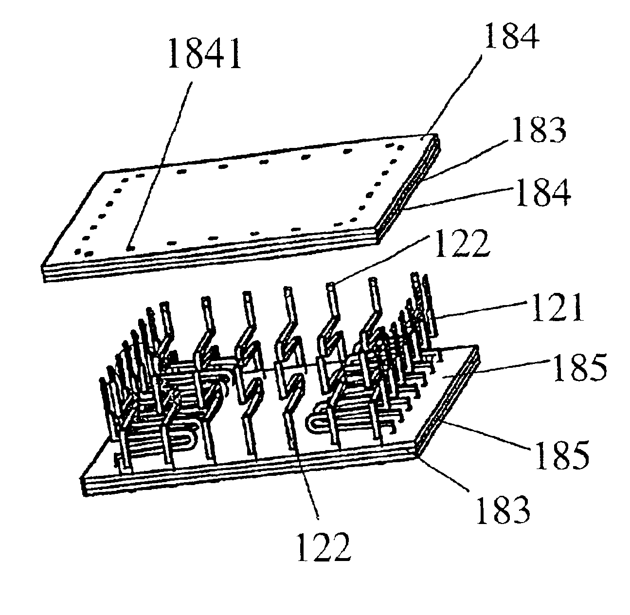
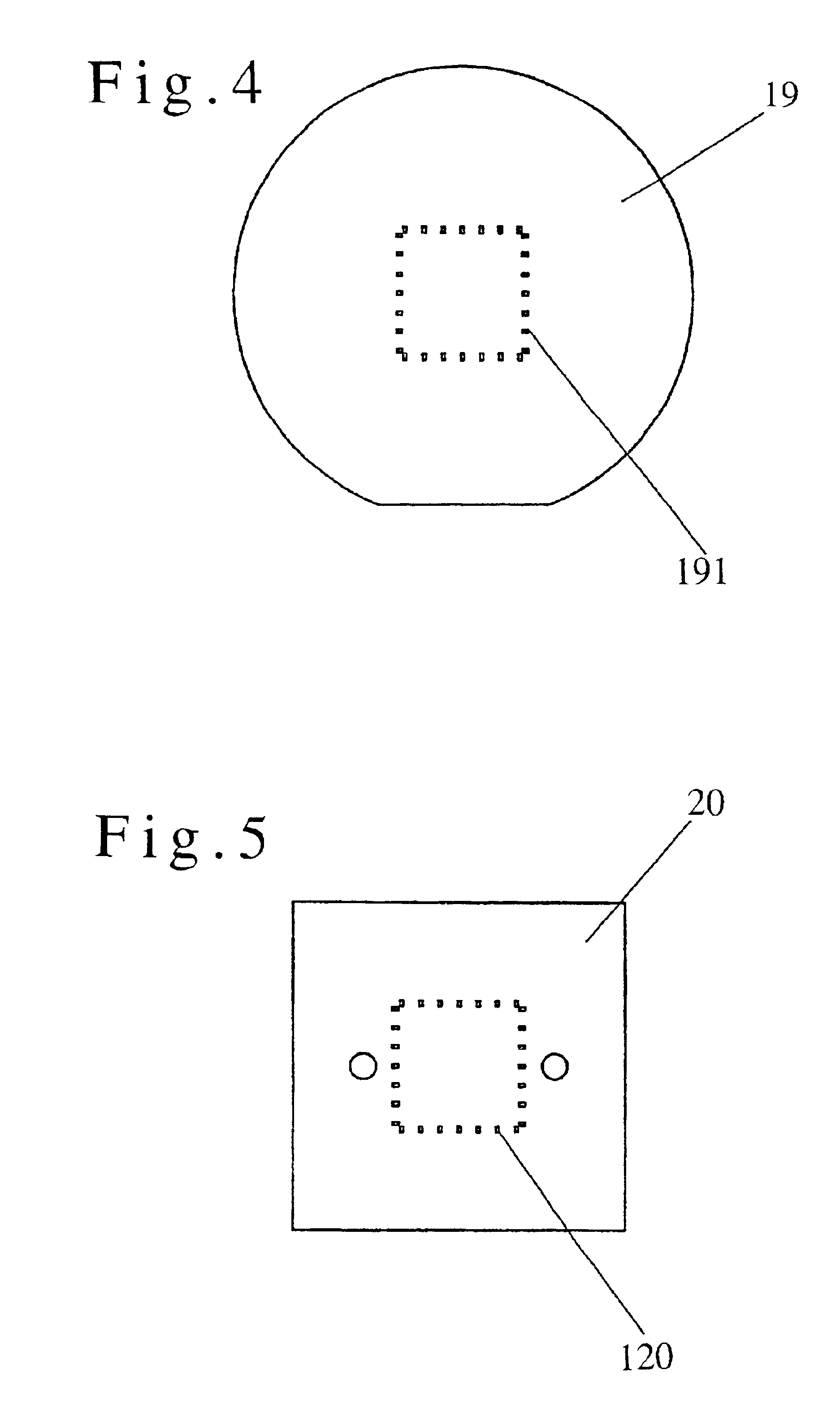
FIGS. 4-21 illustrate a first embodiment of the present invention. FIG. 4 shows an array of electrode pads on a wafer, while FIG. 5 shows an array of electrode pads on a circuit. Referring now to FIG. 4, electrode pads 191 are arrayed on a wafer 19 in one rectangular line. There are some regions in the four corners where electrode pads are absent. As shown in FIG. 5, electrode pads 120 are arrayed on a rectangular line on a circuit board 20. The electrode pads 191 for a single chip on the wafer 19 are located so that they face those of the electrode pads 120 on the circuit board 20 when they are opposed to each other. The first embodiment will describe a probe pin assembly that is suitable for use in establishing electric connection or electric continuity between such opposing electrode pads. Referring now to FIG. 6, the probe pin assembly has a lateral array of parallel probe pins 121 having a plurality of first perpendicular-type probe pins 112 and a vertical array o...

embodiment 2

(Embodiment 2)

FIGS. 22-27 illustrate a second embodiment of the present invention. The second embodiment is the case in which electrode pads are arranged in a staggered pattern.

In FIG. 22, each of the first and second perpendicular-type probe pins 112, 212 is composed of a pair of an outer probe pin 22 and an inner probe pin 21, opposed to the electrode pad 191. Namely, the input unit 13 and the beam extending from the output unit 14 to the deformation unit 15 of the perpendicular-type probe pin 112 (212) opposing the outer electrode pad 191 in the staggered pattern is directed to the outer electrode pad 191 arranged on a rectangular line, while the input unit 13 and the beam extending from the output unit 14 to the deformation unit 15 of the perpendicular-type probe pin 112 (212) opposing the inner electrode pad 191 in the staggered pattern is directed to the inner electrode pad 191 arranged on a rectangular line. As shown in FIG. 23, the principle structures of the input unit 13, ...


PUM


Abstract

A prove pin assembly is provided in which the probe pins for a chip under test occupy the only space above the chip, not extending into the space above the adjacent chip. The probe pin assembly has a lateral array of parallel probe pins of a plurality of first perpendicular-type probe pins and a vertical array of parallel probe pins of a plurality of second perpendicular-type probe pins, wherein said lateral array of parallel probe pins and vertical array of parallel probe pins occupy different spaces for deformation above the region of the chip under test and fit in the limited planar range corresponding to the chip.

Description

BACKGROUND OF THE INVENTION1. Field of the InventionThis invention relates to probe pin assemblies for use in the electric measurement of semiconductor integrated circuit chips and liquid crystal devices, more specifically, to a probe pin assembly for use in testing integrated circuits on a wafer.2. Description of Prior ArtConventionally, the electric properties of a chip such as an IC chip and LSI chip are measured by contacting probe pins to the chip terminals for electric continuity. Cantilever type probe pins and perpendicularly movable pins are typical examples. In the cantilever type probe pin assembly, the probe pins are arrayed horizontally over the substrate and the pin ends are connected to the circuit pattern on a substrate. In the perpendicularly movable probe pin assembly, the probe pins are mounted vertically on the substrate and their output ends are connected to the circuit pattern on the substrate. Both types of pin probe assemblies adopt the beam structure to provi...

Claims


Application Information

Patent Timeline
Patent Type & Authority Patents(United States)
IPC IPC(8): G01R1/067G01R1/073G01R31/26G01R1/06H01L21/66
CPCG01R1/06738G01R1/07357G01R1/07314G01R1/06727G01R1/073
Inventor KIMOTO, GUNSEITAKAI, SHINKICHI
Owner KIMOTO GUNSEI
Why Eureka
Try Eureka