Differential charge pump circuit

a charge pump and charge circuit technology, applied in pulse automatic control, pulse technique, instruments, etc., can solve the problems of mismatches between isub>cmr /sub>and isub>cml /sub>in semiconductor manufacturing processes, and the inability to generate slicing signals with digital sum equal to 0, so as to eliminate the influence of mismatches

Inactive Publication Date: 2005-01-25
MEDIATEK INC
View PDF6 Cites 25 Cited by
  • Summary
  • Abstract
  • Description
  • Claims
  • Application Information

AI Technical Summary

Benefits of technology

One aspect of the present invention is to provide a differential charge pump circuit for eliminating influence of mismatches between common mode current sources and keeping an output voltage having a 50% duty cycle. The differential charge pump circuit includes a capacitor, a slicer, a first current source, a second current source, a first-common-mode current source, a second-common-mode current source, and a third-common-mode current source. The capacitor has a first terminal and a second terminal and provides an output voltage. The slicer outputs a comparison signal to control a charge/discharge action of the capacitor. The first current source includes a positive terminal and a negative terminal. The positive terminal is connected to a positive reference voltage. The negative terminal is connected to the first terminal of the capacitor when the comparison signal is H, and to the second terminal of the capacitor when the comparison signal is L. The second current source includes a positive terminal and a negative terminal. The negative terminal of t

Problems solved by technology

However, the slicing out signals with digital sum value equal to 0 can not be generated owing to that there are some mismatches between the currents Iup and Idn.
However, there will be some mismatches between ICMR and ICML in the semiconductor manufacturing pr

Method used


Image

  • Differential charge pump circuit
  • Differential charge pump circuit
  • Differential charge pump circuit

Examples


Embodiment Construction

The differential charge pump circuit of the present invention will be described with reference to the accompanying drawings.

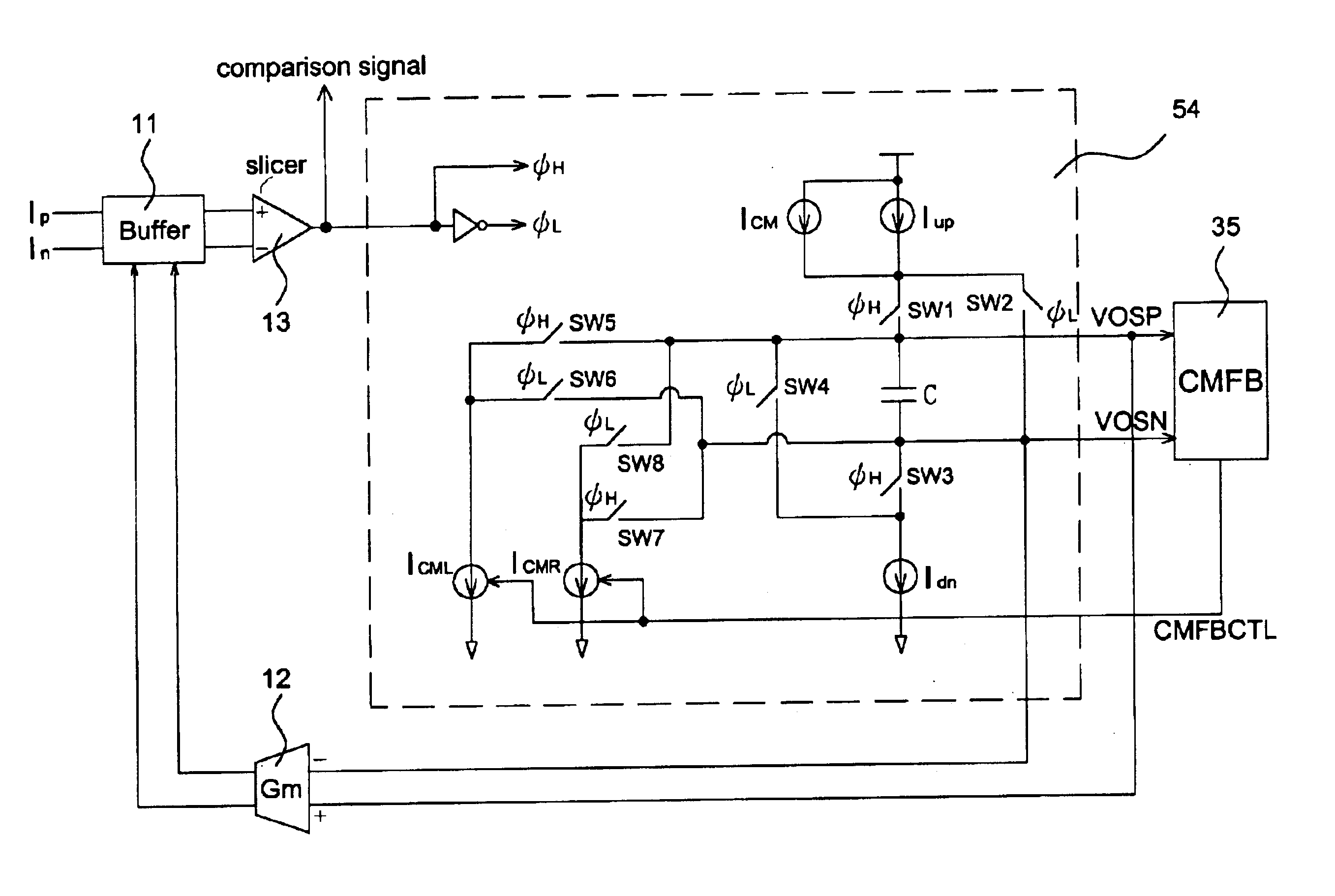
FIG. 5 shows the differential charge pump circuit in accordance with a first embodiment of the present invention. As shown in this drawing, the differential charge pump 54 is the same as a general differential charge pump (as shown in FIG. 3) in that a slicer 13 is used to generate a comparison signal to switch the charge and discharge paths of each current source with respect to the floating capacitor C. The conventional differential charge pump only switches the charge and discharge paths of the upper charging current source Iup and the lower discharging current source Idn with respect to the floating capacitor C. The differential charge pump 54 of this present invention, however, switches not only the charge and discharge paths of the upper charging current source Iup and the lower discharging current source Idn with respect to the capacitor C, but also the ...


PUM


Abstract

A differential charge pump circuit for eliminating influence of mismatches between current sources is disclosed. The differential charge pump circuit includes a floating capacitor for providing an output voltage, a slicer for outputting a comparison signal to control a charge/discharge actions of the floating capacitor, a first current source, a second current source, a first-common-mode current source, a second-common-mode current source, and a third-common-mode current source connected in parallel with the first current source. The differential charge pump circuit of the present invention utilizes switches to switch the charge and discharge current paths of the capacitor with respect to the common mode current source and the charge/discharge current source. Therefore, the duty cycle of the output signal is free from being adversely influenced by the mismatches between the current sources.

Description

BACKGROUND OF THE INVENTIONA. Field of the InventionThe invention relates to a differential charge pump circuit, and more particularly, to a differential charge pump circuit using a method of exchanging common mode current sources to decrease the influence of the mismatches between the common mode currents upon the duty cycle.B. Description of the Related ArtIn the applications of optical storage, the data patterns are embossed on the disk. The embossed pattern signals of the disk are read out by a photo detector and is translated into a voltage signal named RF signal. The RF signal are processed through an automatic gain control circuit, an equalizer circuit and a buffer circuit and then is fed to a slicer circuit to slice data as high or low. The signals after the slicer are bit stream patterns with 1 or 0. If the data “1” is weighted 1 and the data “0” is weighted −1, due to the data format of the disk, the digital sum value (DSV) is equal to 0 for long term. The total numbers of...

Claims


Application Information

Patent Timeline
IPC IPC(8): H03K3/0231H03K3/011H03K3/00H03K3/017H03K3/013
CPCH03K3/011H03K3/0231H03K3/017H03K3/013
Inventor KAO, HSUEH-WU
Owner MEDIATEK INC
Why Eureka
Try Eureka