Method and apparatus for measuring the shape and thickness variation of polished opaque plates

a technology of opaque plate and shape variation, applied in the direction of measurement device, semiconductor/solid-state device testing/measurement, instruments, etc., can solve the problems of insufficient height accuracy and spatial resolution, insufficient height accuracy, and insufficient height accuracy for future wafer requirements

Inactive Publication Date: 2005-01-25
PHASE SHIFT TECH
View PDF10 Cites 88 Cited by
  • Summary
  • Abstract
  • Description
  • Claims
  • Application Information

AI Technical Summary

Benefits of technology

In a more specific embodiment of the invention, the interferometer channels are Fizeau interferometers; and synchronization of the wavelength shifting of light is provided by utilizing a single light source, the output beam of which is spl

Problems solved by technology

For capacitive sensors, the achievable height accuracy and spatial resolution are limited and are no longer adequate for future wafer requirements.
While the spatial resolution is better, the height accuracy is not sufficient.
In addition, the scanning time per wafer is very long for high spatial resolution.
The shortcomings of this technique are that highly doped wafers are not transparent, even in the infrared and cannot be measured, and that only the thickness variation, but not the shape, is obtained.
This technique suffers from the need to place the wafer close to the reference surface, which leads to significant difficulties in wafer handling.
Furthermore, using large angles of incidence of the illumination leads in effect to a desensitizing of the measurement, thus reducing measurement precision.
In addition, it is difficult to combine the two single-sided surface maps to calculate the thickness variation and shape with the necessary overlay accuracy.
The drawbacks here are the requirement for optical components much larger than the wafer, a desen

Method used


Image

  • Method and apparatus for measuring the shape and thickness variation of polished opaque plates
  • Method and apparatus for measuring the shape and thickness variation of polished opaque plates
  • Method and apparatus for measuring the shape and thickness variation of polished opaque plates

Examples


Embodiment Construction

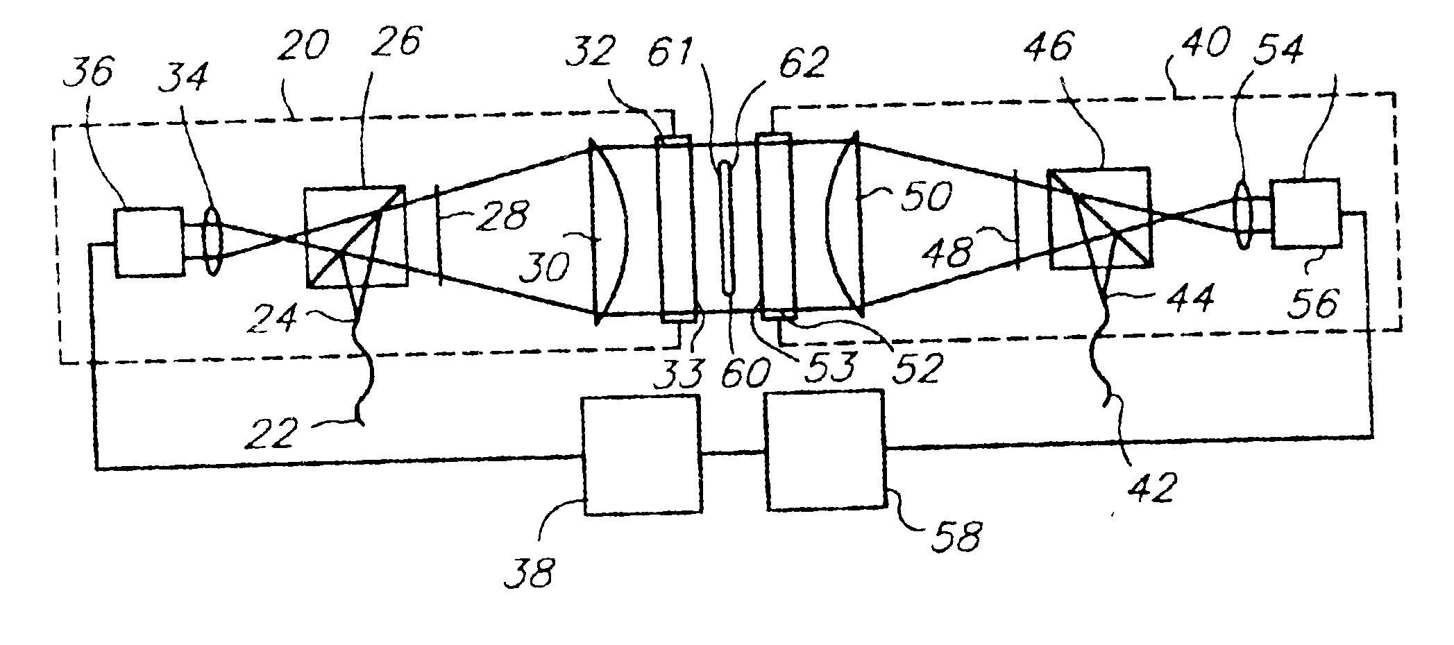
Reference now should be made to the drawings, in which the same reference numbers are used throughout the different figures to designate the same or similar components. Prior to entering into a discussion of the drawings, however, a brief overview of some of the challenges present in providing thickness variation measurements of very thin opaque plates, such as semiconductor wafers, is considered to be in order.

Currently, semiconductor wafers for which surface mapping or profiling of the opposite surfaces is desired, along with a measurement of thickness variation over the entire wafer, requires obtaining such measurements for wafers which have a diameter between 200 mm and 300 mm with a thickness on the order of 750 microns. To obtain rapid measurements of the thickness variation and shape of such thin wafers at the highest accuracy levels and high spatial resolution, double-sided interferometric metrology with its non-contact operation, high resolution due to the short wavelength ...


PUM


Abstract

The present invention consists of a technique and device for measuring the thickness variation and shape of wafers or other polished opaque plates. A combination of two improved phase-shifting Fizeau interferometers is used to simultaneously measure the single-sided distance maps between each side of the wafer and the corresponding reference flat, with the thickness variation and shape being calculated from these data. Provisions are made to determine and eliminate the shape and tilt of the reference surfaces, and also to facilitate the correct overlay of the two single-sided measurements for the calculation of thickness variation and shape.

Description

BACKGROUNDThin polished plates in the form of silicon wafers are a very important part of modern technology. The requirements for flatness and thickness uniformity of these wafers are becoming more and more stringent as the printed device feature sizes are shrinking. Therefore, the metrology of these parameters is very important for development and manufacturing. Other examples for opaque polished plates are magnetic disc substrates, gauge blocks, and the like. While the technique described here refers mainly to wafers, it is to be understood that the technique also is applicable to other types of test pieces with comparable characteristics.There exist a variety of techniques to address the measurement of shape and thickness variation of wafers. Currently, the technique most commonly used is based on capacitive distance sensors (ASTM standards F 1530-94 and F 1390-97). For measurement, two sensors are placed near either side of the wafer and scanned together across the wafer surface...

Claims


Application Information

Patent Timeline
IPC IPC(8): G01B11/30G01B11/06G01B11/00G01B11/24H01L21/66
CPCG01B11/06G01B11/30G01B9/02021G01B9/02027G01B9/02028G01B2290/45
Inventor FREISCHLAD, KLAUSTANG, SHOUHONG
Owner PHASE SHIFT TECH
Why Eureka
Try Eureka