Method for operating NOR type flash memory device including SONOS cells

a technology of flash memory and sonos cells, which is applied in the direction of digital storage, transistors, instruments, etc., can solve the problems of difficult high-integration of memory devices, and achieve the effect of high-integration

Inactive Publication Date: 2005-01-25
SAMSUNG ELECTRONICS CO LTD
View PDF3 Cites 46 Cited by
  • Summary
  • Abstract
  • Description
  • Claims
  • Application Information

AI Technical Summary

Benefits of technology

According to the present invention, provided can be a method for operating a flash memory device in whic

Problems solved by technology

Also, it is difficult to high

Method used


Image

  • Method for operating NOR type flash memory device including SONOS cells
  • Method for operating NOR type flash memory device including SONOS cells
  • Method for operating NOR type flash memory device including SONOS cells

Examples


Embodiment Construction

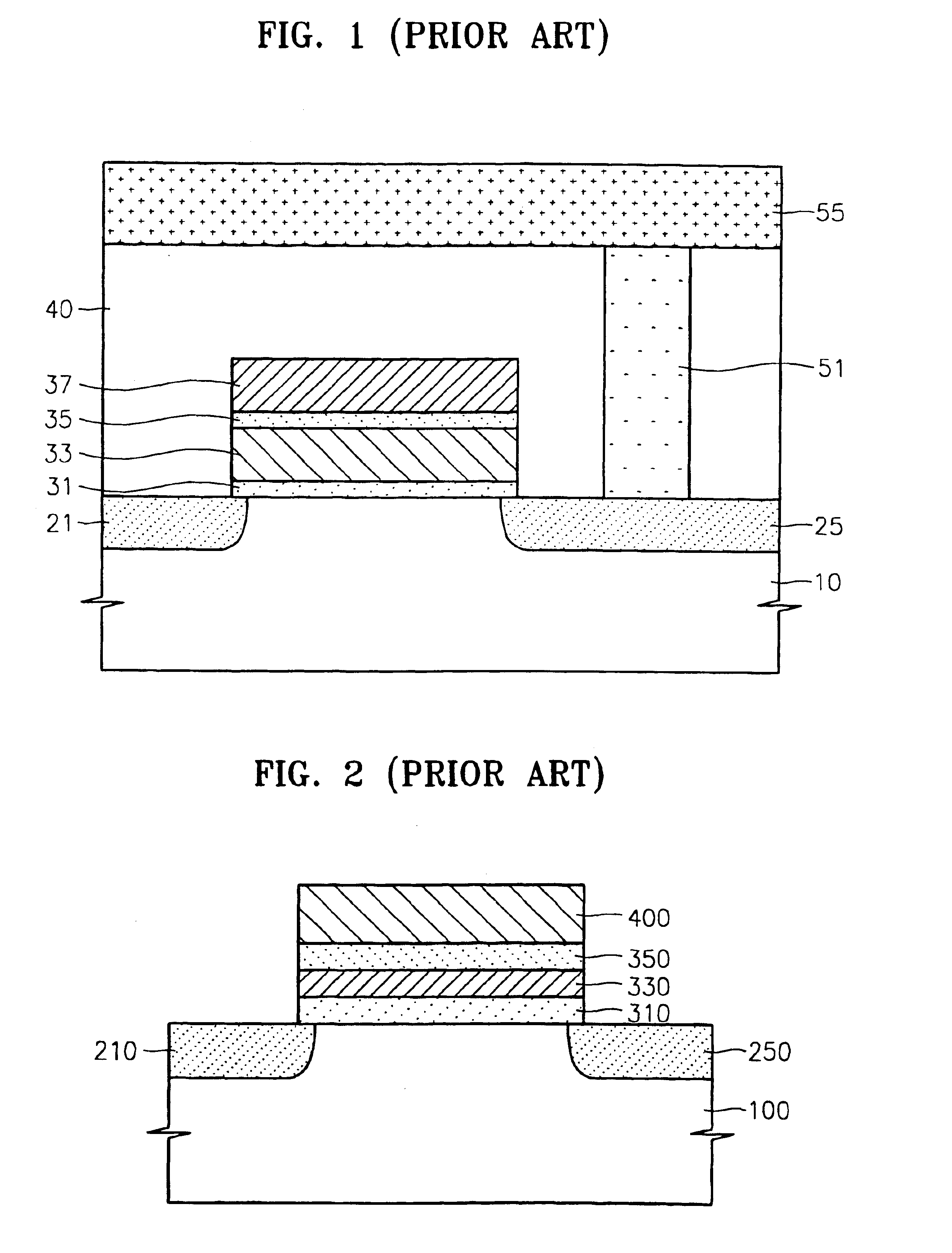
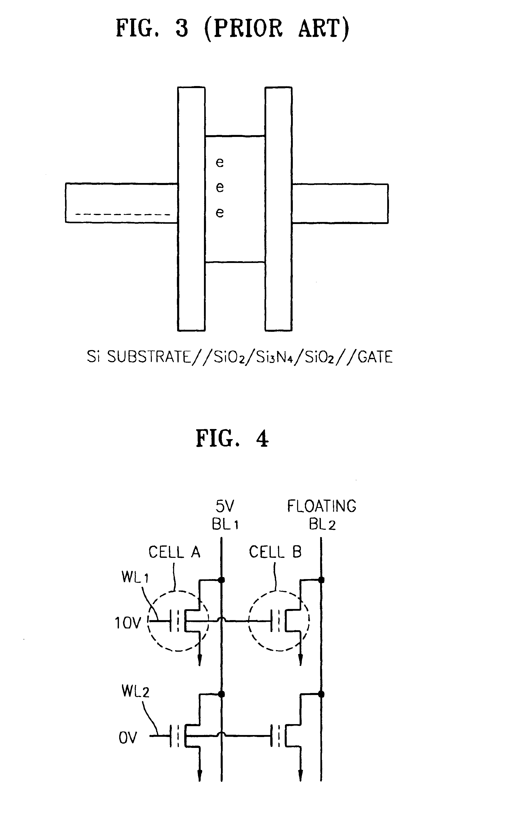
Hereinafter, embodiments of the present invention will be described in detail with reference to the attached drawings. However, the embodiments of the present invention can be modified into various other forms, and the scope of the present invention must not be interpreted as being restricted to the embodiments. The embodiments are provided to more completely explain the present invention to those skilled in the art. In drawings, the thicknesses of layers or regions are exaggerated for clarity. Like reference numerals in the drawings denote the same members. Also, when it is written that a layer is formed “on” another layer or a substrate, the layer can be formed directly on the other layer or the substrate, or other layers can intervene therebetween.

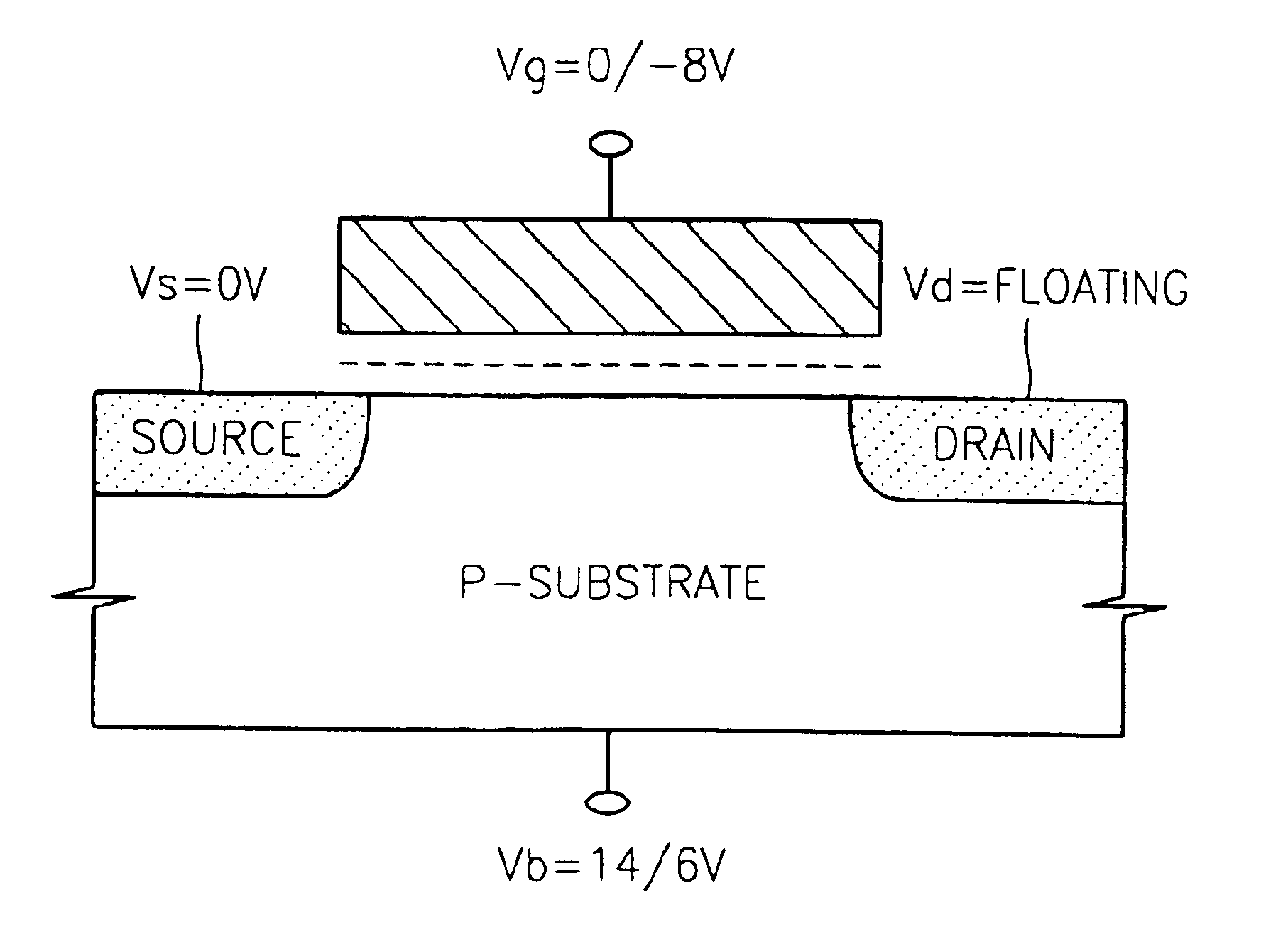
In embodiments of the present invention, silicon-oxide-nitride-oxide-semiconductor (SONOS) cells are used as unit cells in a NOR-type flash memory device. A solution to problems, which must be solved before the NOR-type flash memory dev...


PUM


Abstract

Provided is a method for operating a NOR-type flash memory device using SONOS cells. The SONOS cells are selectively programmed using channel hot electron injection and erased using Fowler-Nordheim tunneling and hot hole injection. When the SONOS cells are programmed, a voltage within a range of 8V-12V is applied to a selected word line and a voltage within a range of 3V-6V is applied to a selected bit line. When the SONOS cells are erased, the selected word line is ground and a voltage within a range of 13V-18V is applied to a substrate. Alternatively, a voltage of about −8V is applied to the selected word line, a voltage of about 6V is applied to the substrate, and a bit line and a source line float.

Description

BACKGROUND OF THE INVENTIONThis application claims the priority of Korean Patent Application No. 2002-73815 filed on Nov. 26, 2002 in the Korean Intellectual Property Office, the disclosure of which is incorporated herein in its entirety by reference.1. Field of the InventionThe present invention relates to a nonvolatile memory device, and more particularly, to a method for operating a NOR-type flash memory device having silicon-oxide-nitride-oxide-semiconductor (SONOS) cells.2. Description of the Related ArtNonvolatile semiconductor memory devices can have a variety of types which have a common characteristic in that after an applied power is removed from the nonvolatile semiconductor memory devices, the nonvolatile semiconductor memory devices can retain stored information. Of such nonvolatile semiconductor memory devices, a flash memory device can be largely classified into a NAND-type flash memory device and a NOR-type flash memory device according to the array form of unit cell...

Claims


Application Information

Patent Timeline
IPC IPC(8): G11C16/16G11C16/10G11C16/04G11C16/06H01L21/8247H01L27/115H01L29/788H01L29/792
CPCG11C16/0466G11C16/16G11C16/10H10B69/00
Inventor CHO, MYOUNG-KWAN
Owner SAMSUNG ELECTRONICS CO LTD
Why Eureka
Try Eureka