Semiconductor dynamic sensor

Inactive Publication Date: 2005-02-01
DENSO CORP
View PDF16 Cites 23 Cited by
  • Summary
  • Abstract
  • Description
  • Claims
  • Application Information

AI Technical Summary

Benefits of technology

The present invention has been made in view of the above-mentioned problem, and an object of the present invention is to provide an improved semiconductor dynamic sensor, in which a sensor chip is correctly mounted on a substrate such as

Problems solved by technology

However, it is difficult to exactly position the sensor chip on the circuit chip at a predetermined position, because the adhesi

Method used


Image

  • Semiconductor dynamic sensor
  • Semiconductor dynamic sensor
  • Semiconductor dynamic sensor

Examples


Embodiment Construction

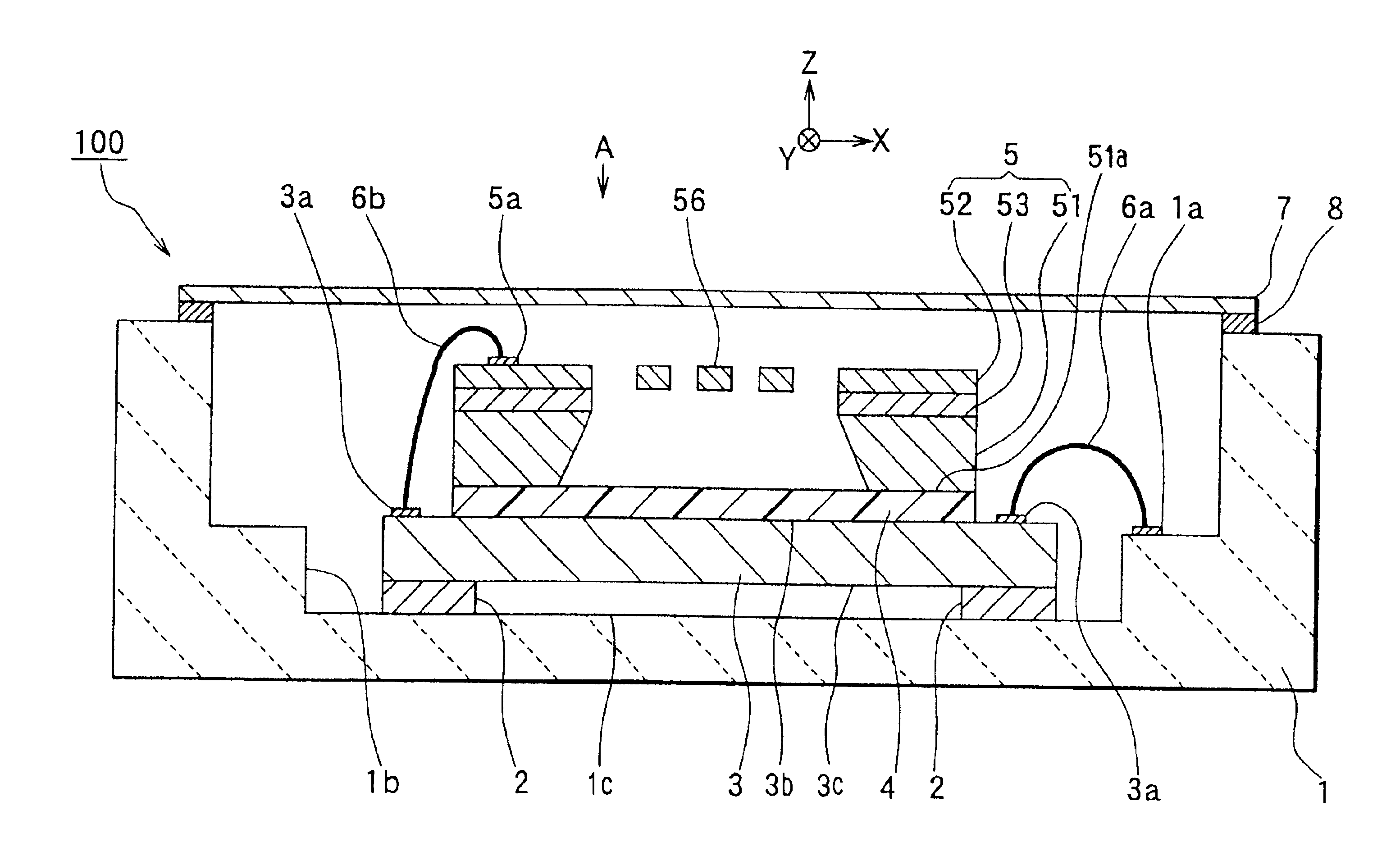
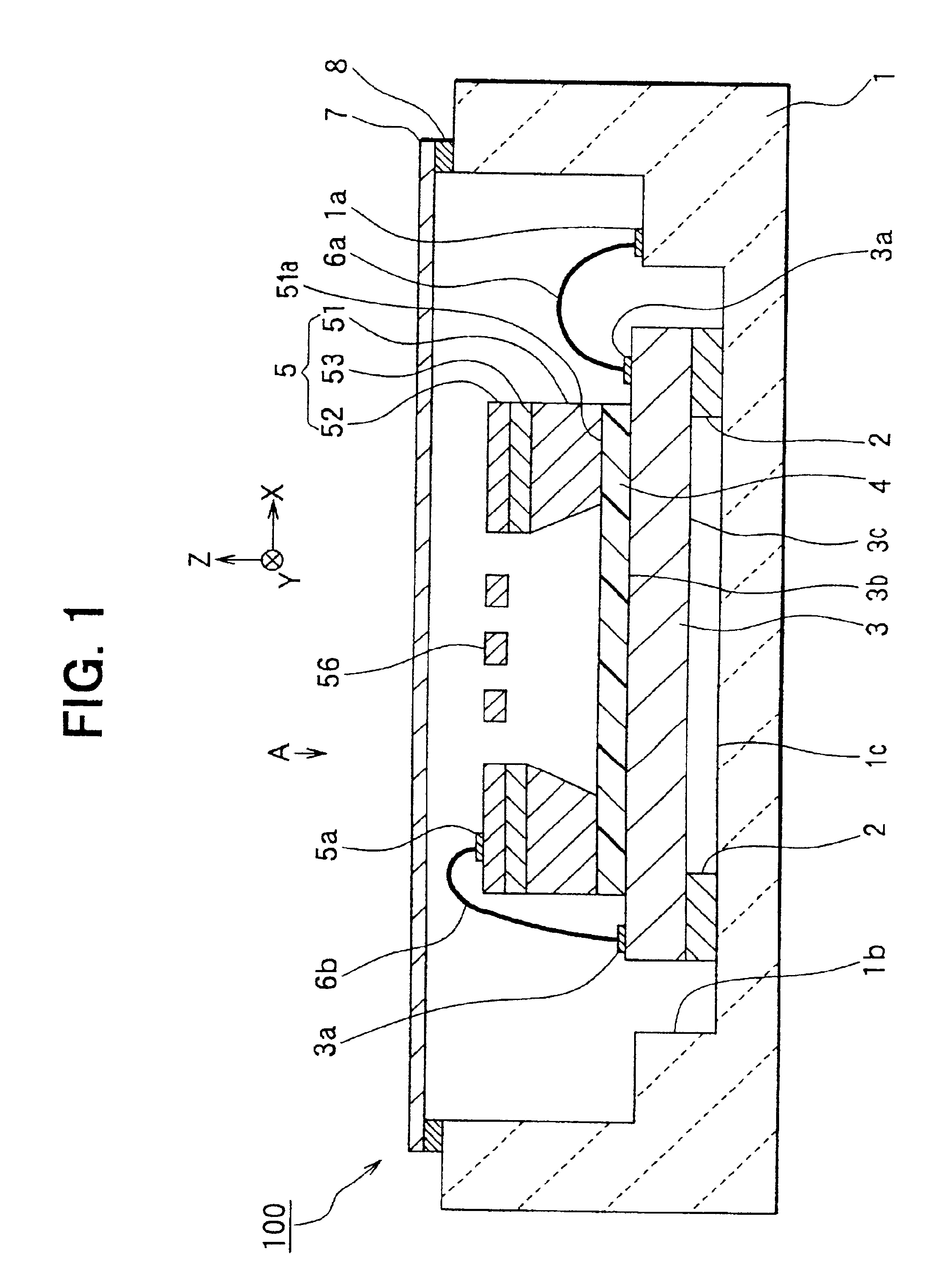
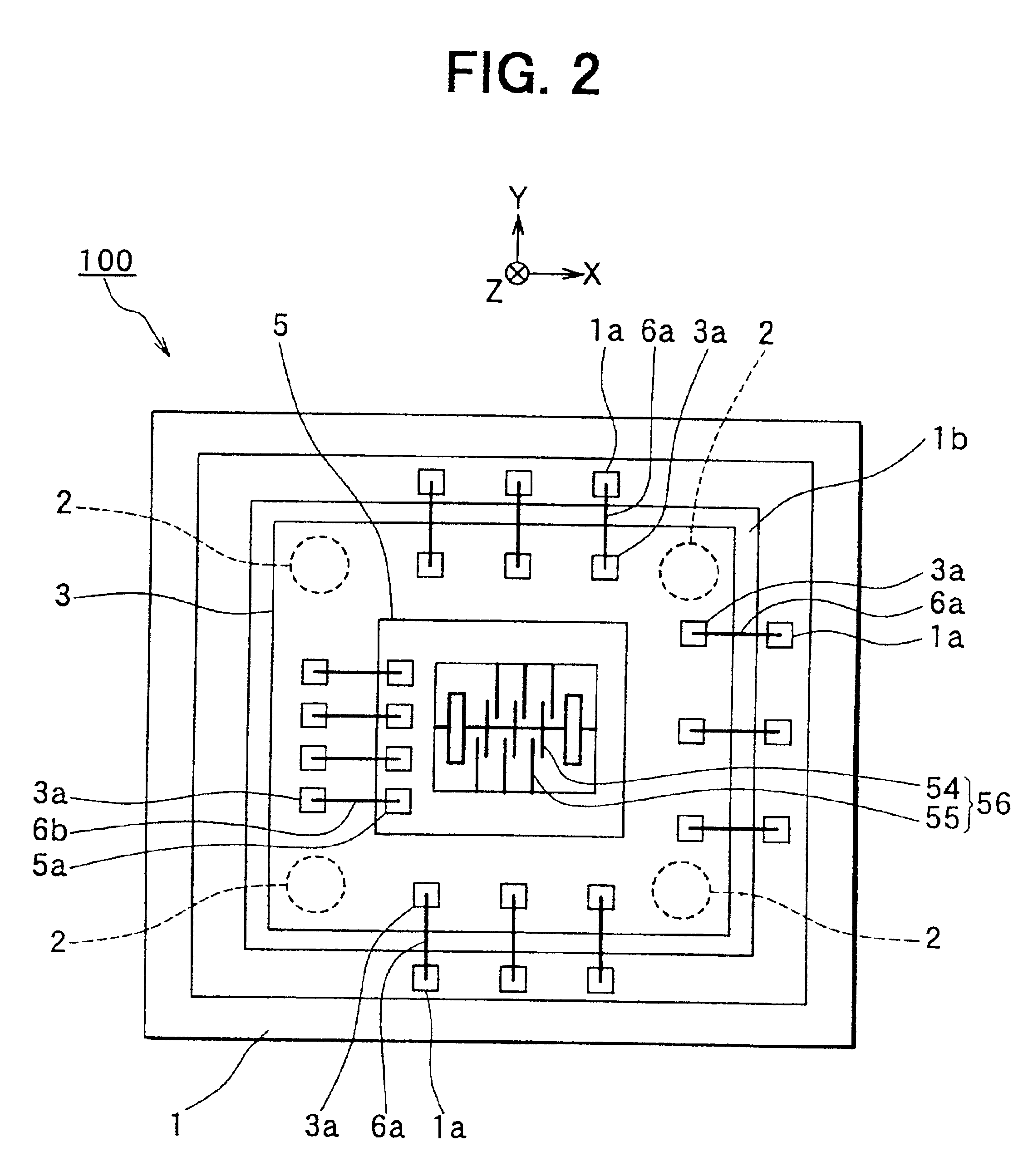
An embodiment of the present invention will be described with reference to FIGS. 1 and 2, showing a cross-sectional view and a plan view of an semiconductor acceleration sensor 100, respectively. FIG. 2 shows a plan view viewed in direction A shown in FIG. 1 with a cover plate removed. The acceleration sensor 100 is composed of a semiconductor sensor chip 5 and a substrate 3 both contained in a package case 1.

The package case 1 is made of ceramics, and a cavity 1b for containing the sensor chip 5 and the substrate 3 therein is formed in the package case 1. The substrate 3, which is a semiconductor IC-chip having a circuit for processing sensor signals (referred to as a circuit chip), is mounted on a mounting surface 1c in the cavity 1b via adhesive 2. The semiconductor sensor chip 5 is mounted on the circuit chip 3 via an adhesive film 4. Pads 1a, 3a and 5a made of aluminum or the like for wire-bonding are formed on the package case 1, the circuit chip 3 and the sensor chip 5, respe...


PUM


Abstract

A semiconductor dynamic sensor such as an acceleration sensor is composed of a sensor chip having electrodes movable in response to acceleration applied thereto and a circuit chip having a circuit for processing signals fed from the sensor chip. The sensor chip and the circuit chip are contained and held in a packaging case. The sensor chip and the circuit chip are fixedly connected via an adhesive film. The sensor chip is correctly positioned on the circuit chip without creating misalignment relative to a sensing axis, because the adhesive film from which an adhesive material does not flow out under heat is used. A semiconductor wafer including plural sensor chips is first made and the adhesive film is stuck to one surface of the wafer, and then individual sensor chips are separated by dicing. The sensor chip is connected to the circuit chip via the adhesive film.

Description

CROSS-REFERENCE TO RELATED APPLICATIONThis application is based upon and claims benefit of priority of Japanese Patent Application No. 2000-191535 filed on Jun. 26, 2000, the content of which is incorporated herein by reference.BACKGROUND OF THE INVENTION1. Field of the InventionThe present invention relates to a semiconductor dynamic sensor such as an acceleration sensor which includes a semiconductor sensor chip for generating signals according to a dynamic force applied thereto and a substrate for mounting the sensor chip thereon.2. Description of Related ArtAn example of an acceleration sensor is disclosed in JP-A-8-110351. This acceleration sensor includes a semiconductor sensor chip having a movable member for generating a sensor signal according to acceleration applied thereto. The sensor chip is attached and connected to a circuit chip for processing the sensor signal with an adhesive material. The acceleration sensor is made compact in size by laminating the sensor chip on ...

Claims


Application Information

Patent Timeline
IPC IPC(8): B81B7/00G01P1/02G01P15/125G01P1/00G01P15/08H01L29/84
CPCB81C1/00333G01P1/023G01P15/125H01L2224/48091H01L2224/48227G01P2015/0814H01L2924/01039H01L2924/01079H01L2224/73265H01L2924/00014
Inventor KUNDA, TOMOHITO
Owner DENSO CORP
Why Eureka
Try Eureka