Semiconductor memory device having mode storing one bit data in two memory cells and method of controlling same

a memory device and semiconductor technology, applied in information storage, static storage, digital storage, etc., can solve the problems of affecting normal access, affecting the normal operation of the device, and affecting the ability to refresh operations by continuous write operations, so as to suppress the increase in access time and reduce the duration of data copying.

Inactive Publication Date: 2005-02-01
RENESAS ELECTRONICS CORP
View PDF8 Cites 133 Cited by
  • Summary
  • Abstract
  • Description
  • Claims
  • Application Information

AI Technical Summary

Benefits of technology

[0022]Accordingly, it is an object of the present invention to provide a semiconductor memory device and a method of controlling the same that achieve reduction in a data copy duration in the twin cell and suppress an increase in access time due to the refresh operation.
[0023]It is another object of the present invention to provide a semiconductor memory device that makes it possible to write data properly for the twin cell at the time of shifting to the partial mode, and a method of controlling the same. It is further another object of the present invention to provide a semiconductor memory device wherein read / write is possible within a predetermined access time even when switched from a normal mode to a stand-by mode and suddenly received a read / write request while switching to a partial mode, and a method of controlling the same.

Problems solved by technology

In addition, it has been known that an asynchronous pseudo SRAM that does not require external refresh control so that it can operate with completely the same specifications as those of general-purpose SRAMs, suffers from such problems that normal access is affected by refresh operations and that refresh operations become impossible by continuous write operations.
This is because it leads to degradations in access time and cycle characteristics.
Also, even in DRAMs compatible with asynchronous SRAMs in which read / write operations are performed after refreshing as described in the above-mentioned Patent Document 1, it is undesirable to widen the refresh operations since it causes degradation in access time.
Moreover, in terms of performance specifications, it is difficult to widen the time for the refresh operations in a cell array of high-speed synchronous SRAM that is to be incorporated in portable terminals and switching functions and routing functions for networks.

Method used


Image

  • Semiconductor memory device having mode storing one bit data in two memory cells and method of controlling same
  • Semiconductor memory device having mode storing one bit data in two memory cells and method of controlling same
  • Semiconductor memory device having mode storing one bit data in two memory cells and method of controlling same

Examples


Embodiment Construction

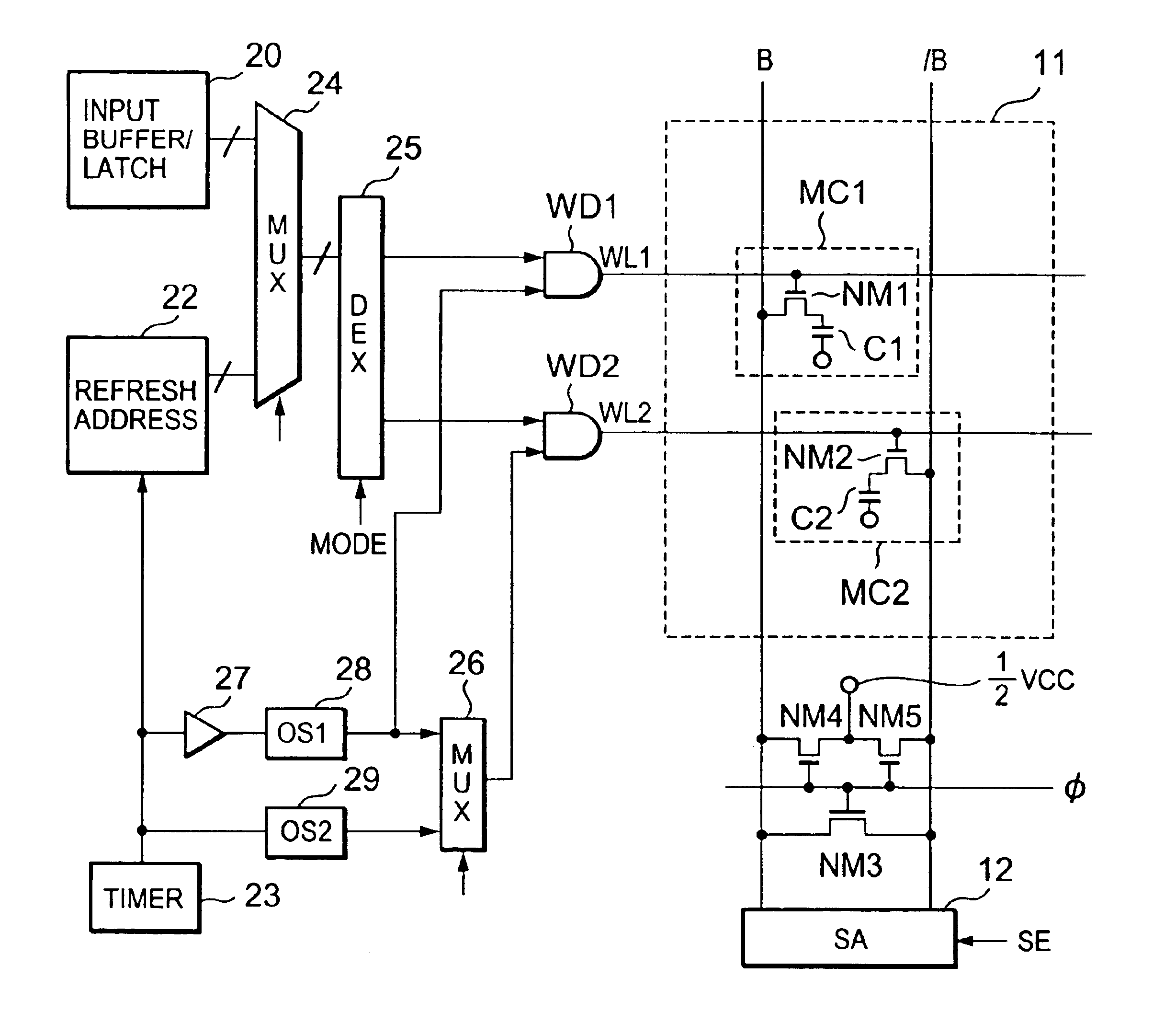
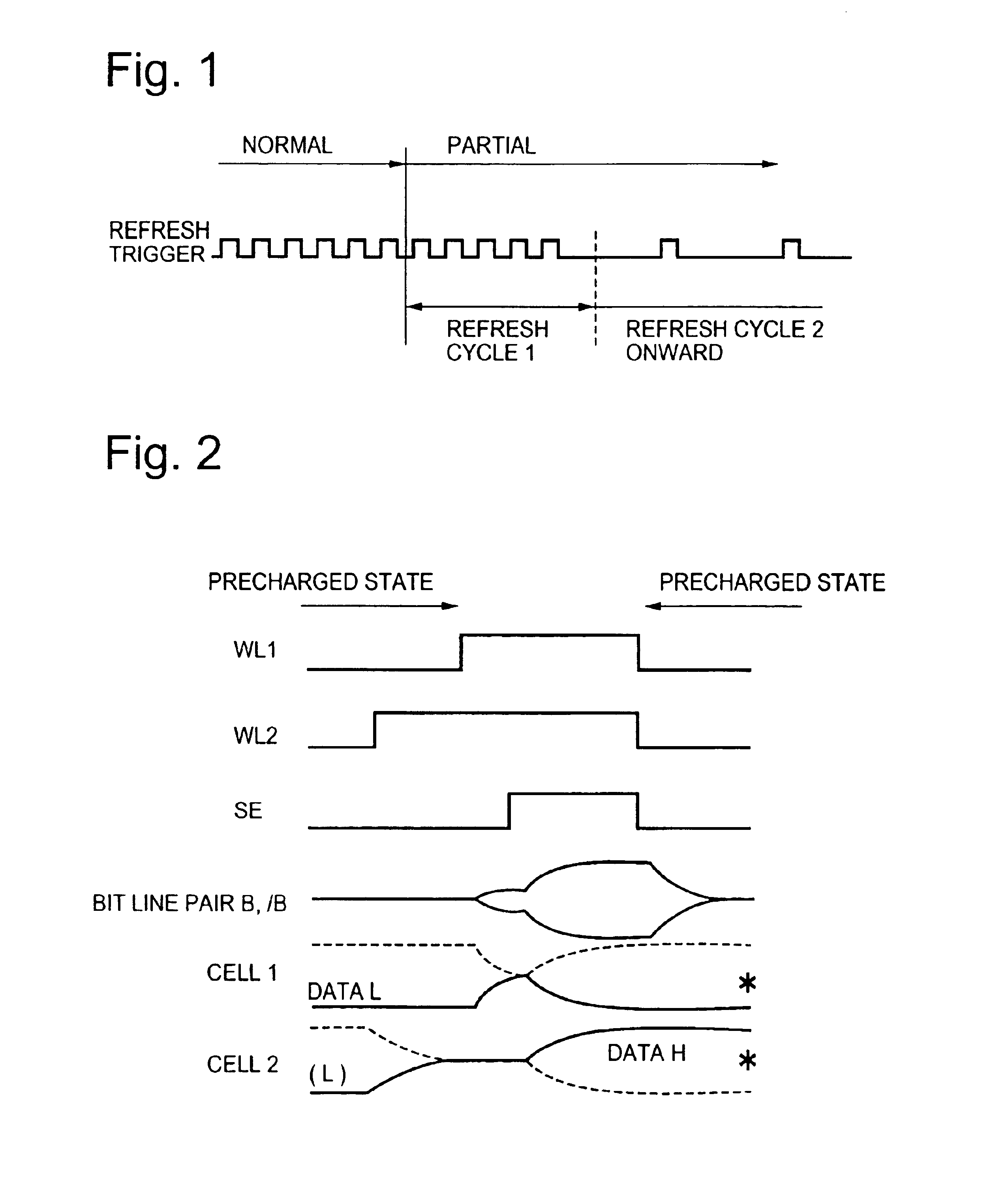
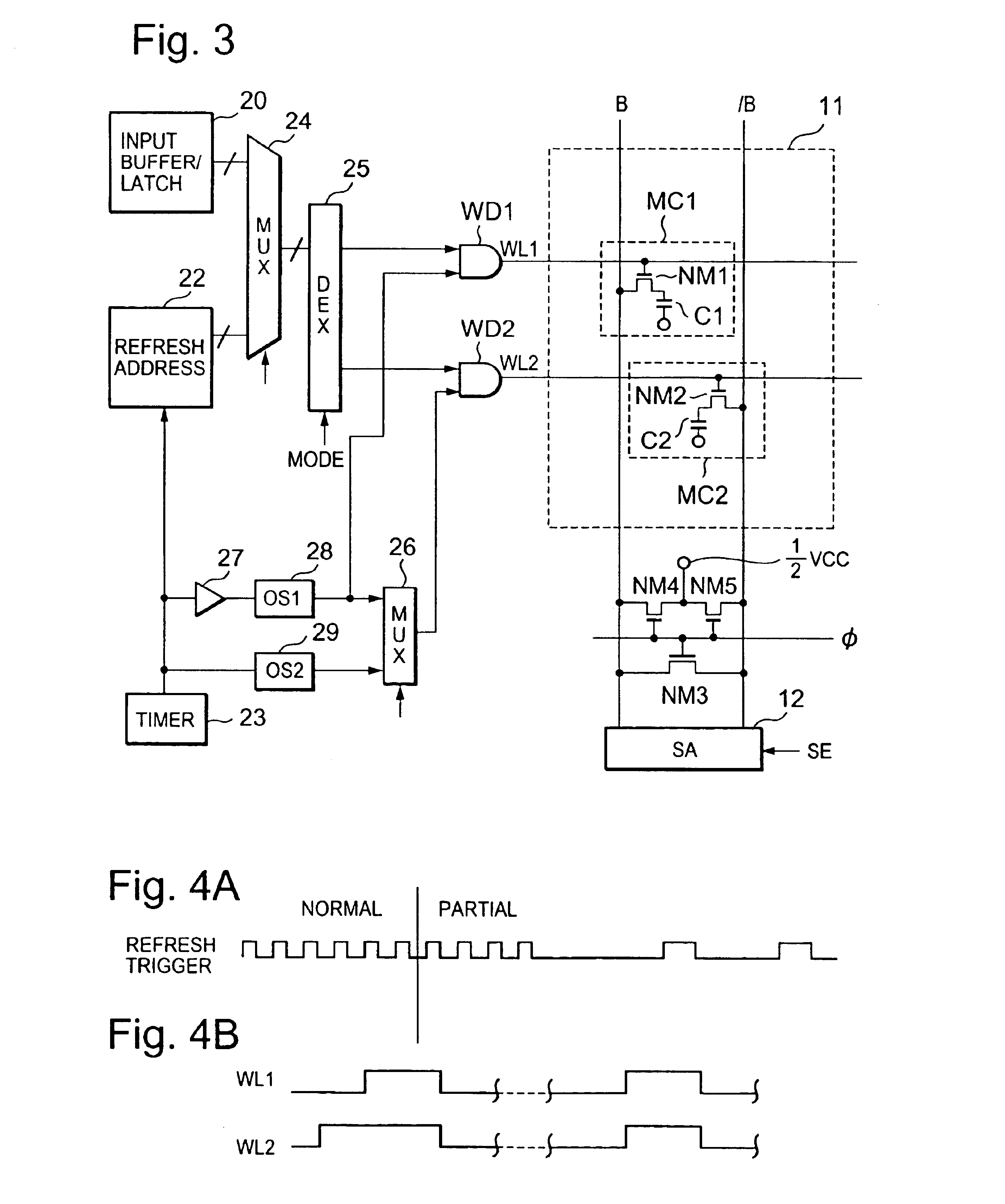
[0042]Preferred embodiments of the present invention are described below. Referring to FIG. 3, in one preferred embodiment, a semiconductor memory device according to the present invention comprises: a cell array (11) having a plurality of memory cells, the cell array including at least; a bit line pair comprising first and second bit lines (B, / B) commonly connected to a sense amplifier (SA); a first memory cell (MC1) including a memory cell transistor (NM1), the gate of which is connected to a first word line (WL1) and one of the drain and source of which is connected to the first bit line (B), and a capacitor element (C1) connected to the other one of the drain and source of the memory cell transistor (MC1); and a second memory cell (MC2) including a memory cell transistor (NM2), the gate of which is connected to a second word line (WL2) and one of the drain and source of which is connected to the second bit line ( / B), and a capacitor element (C2) connected to the other one of th...


PUM


Abstract

A device has a bit line pair including first and second bit lines, a sense amplifier commonly connected to the bit line pair, and first and second cells connected at intersecting portions of first and second word lines and the first and second bit lines. In a normal mode, the first and second word lines are assigned separate addresses, whereas in a partial mode, the first and second word lines are assigned the same address. The first and second cells complimentarily store one bit of data. In storing a data in a first cell of two cells comprised in a twin cell into a second cell when set to the partial mode, the second word line is activated based on a trigger signal generated by a refresh timer during a precharge period for the bit line pair, and subsequently the precharge is completed. The first word line is then activated based on a delayed signal of the trigger signal, and the sense amplifier is activated to amplify a differential voltage between the bit line pair, so that the data of the first cell is written back into the first and second cells.

Description

BACKGROUND OF THE INVENTION[0002]1. Field of the Invention[0003]The present invention relates to a semiconductor memory device and a method of controlling the same, and more particularly to a refresh control for a semiconductor memory device having a mode in which one bit of data is stored by two memory cells.[0004]2. Description of Related Art[0005]It is proposed a method that retains one bit data by using twin memory cell. FIG. 14 is a diagram for explaining such a method. Referring to FIG. 14, a cell array 11 a bit line pair comprising first and second bit lines B and / B which are commonly connected to a sense amplifier (SA) 12, and is provided with a first memory cell MC1 which is connected to a first word line WL1 and the first bit line B, and a second memory cell MC2 which is connected to a second word line WL2 and the second bit line / B. In a normal mode (normal operation) of one bit-one cell, the first and second word lines WL1 and WL2 which are respectively driven by first ...

Claims


Application Information

Patent Timeline
Patent Type & Authority Patents(United States)
IPC IPC(8): G11C11/406G11C11/401G11C11/403
CPCG11C11/406G11C11/40603G11C11/40615G11C2211/4067G11C2211/4061G11C11/401
Inventor TAKAHASHI, HIROYUKI
Owner RENESAS ELECTRONICS CORP
Why Eureka
Try Eureka