Method and apparatus for testing semiconductor wafers

a technology of semiconductor wafers and sample chucks, which is applied in the direction of individual semiconductor device testing, semiconductor/solid-state device testing/measurement, instruments, etc., can solve the problems of inconvenient use, high cost of doing so, and contaminated wafers by contact with these surfaces, so as to ensure the validity of interpolation between test points and not compromise the effect of validity

Inactive Publication Date: 2005-02-01
SOLID STATE MEASUREMENTS
View PDF5 Cites 11 Cited by
  • Summary
  • Abstract
  • Description
  • Claims
  • Application Information

AI Technical Summary

Benefits of technology

Preferably, the tiny openings extending through the semiconductor layer are minimized in number and located relative to the test points in the pattern of test points such that the validity of the interpolation between test points is not compromised. Preferably, the passages in the base structure are located and sized relative to the test points in the pattern of test points such that the validity of the interpolation between test points is not compromised.

Problems solved by technology

Unfortunately, the wafers can be contaminated by contact with these surfaces.
Sample chucks have also been made from pure silicon, but to do so is prohibitively expensive.
One potential drawback to such a sample chuck, however, is that under certain circumstances, variations in the semiconductor top layer may present themselves as variations in the measurement of capacitance-voltage (CV) data, for example.

Method used


Image

  • Method and apparatus for testing semiconductor wafers
  • Method and apparatus for testing semiconductor wafers

Examples


Embodiment Construction

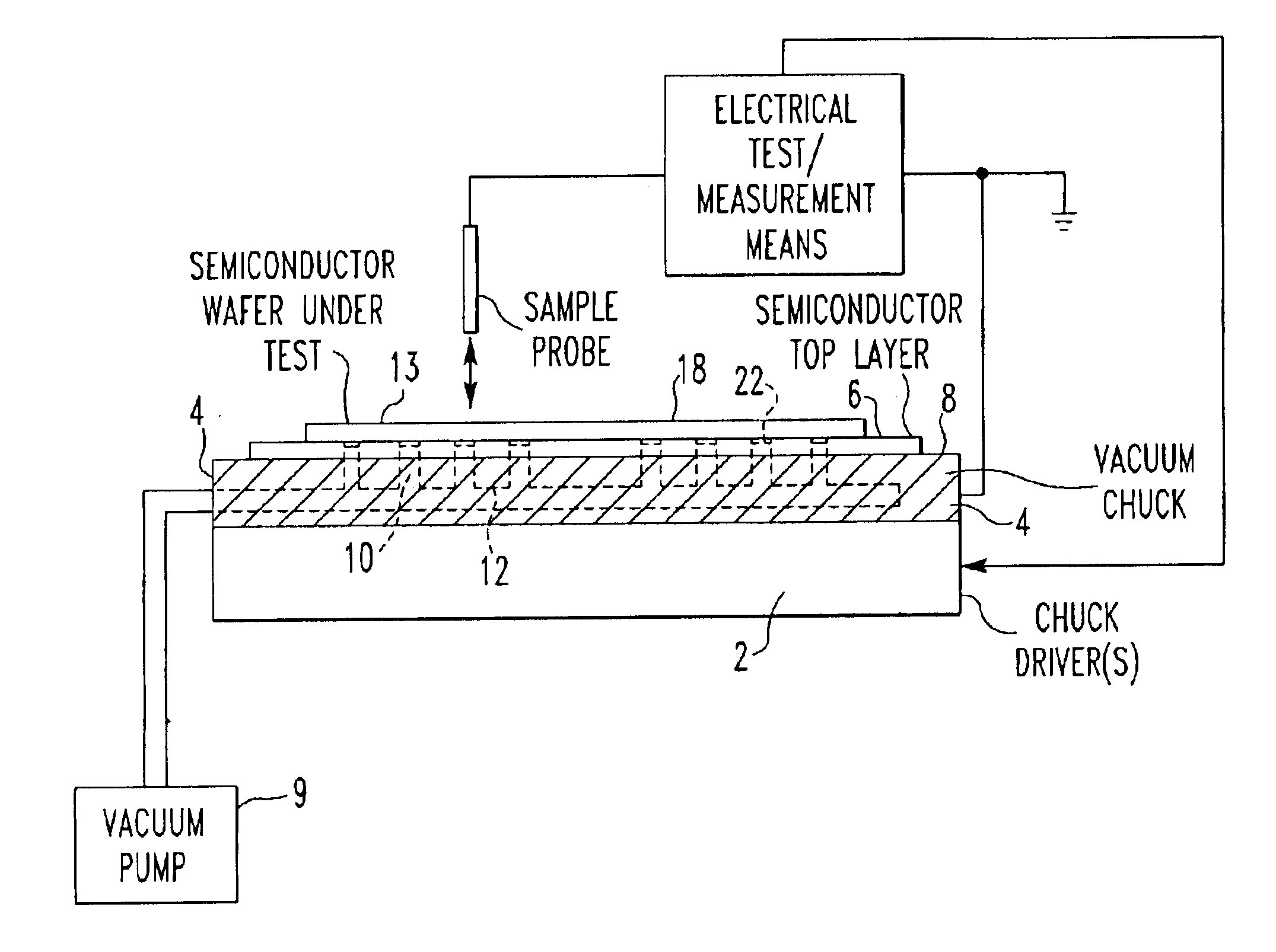
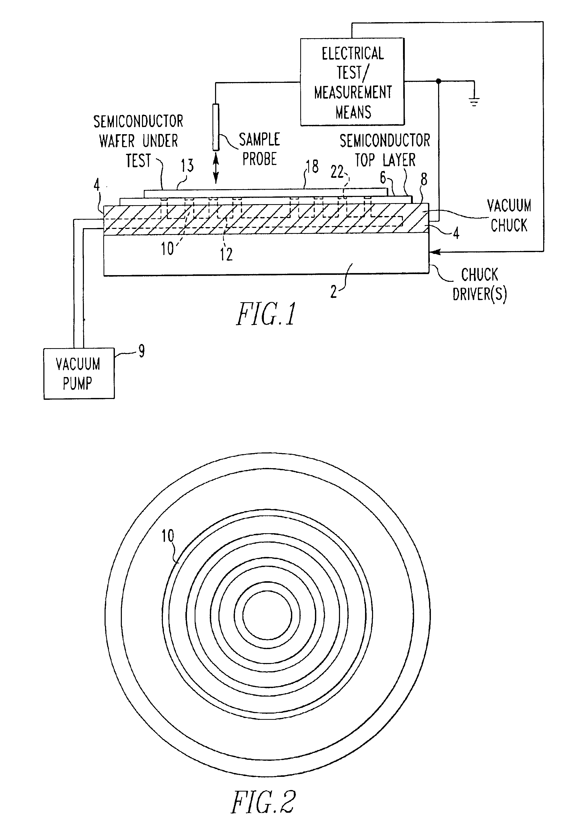
With reference to FIG. 1, a sample chuck 2, in accordance with the present invention, is a laminated structure having a lower layer 4 and an upper layer 6 laminated to a top surface 8 of lower layer 4.

Lower layer 4 is formed from an electrically conductive material, such as aluminum, which provides low mass and weight, acceptable structural rigidity, and ease of manufacturing. One or more vacuum passages or grooves 10 may be formed in top surface 8 for connection to a vacuum source 9 via a vacuum duct 12, shown in phantom, which interconnects one or more vacuum passages 10, shown in phantom, to vacuum source 9. Vacuum source 9, vacuum passages 10, and vacuum duct 12 coact to distribute a vacuum to top surface 8, which can be utilized to secure a semiconductor wafer under test 13 to sample chuck 2.

The conductive material forming lower layer 4 is selected to provide a high quality electrical contact for uniformly distributing electrical current during electrical measurement or other e...


PUM


Abstract

A wafer testing apparatus comprises a sample chuck having a flat surface for supporting a test wafer positioned thereon, the sample chuck having a base structure manufactured of a conductive metal and having a semiconductor layer secured to the base structure defining the flat surface of the sample chuck, an electrical test probe establishing a correction factor corresponding to a location on the semiconductor layer surface to be used to report an electrical property at a location on a test wafer substantially unaffected by the electrical properties of the semiconductor layer and base structure below that location.

Description

BACKGROUND OF THE INVENTION1. Field of the InventionThe present invention relates to a sample chuck for wafers and method of testing wafers mounted on the sample chuck.2. Description of Related ArtSemiconductor wafers are thin, circular slices of doped silicon from which integrated circuits or semiconductor devices are built. Depending on the state of production, the wafers may be referred to as blank wafers, polished wafers, patterned wafers, product wafers, or the like. The largest wafer in current use is 300 mm (12 inch) diameter.At each stage in the integrated circuit manufacturing process, wafers must be carefully inspected for electrical properties that may have values varying over the surface of the wafers. In a typical apparatus for inspecting the electrical properties of a semiconductor wafer, the wafer is supported on a sample chuck or fixture and a probe tip is caused to contact the surface of the semiconductor. A capacitance-voltage (CV), current-voltage (IV), conductanc...

Claims


Application Information

Patent Timeline
Patent Type & Authority Patents(United States)
IPC IPC(8): G01R31/28H01L21/68H01L21/66H01L21/67G01R31/26H01J61/16H01J61/20H01J61/33H01J61/88
CPCG01R31/2831H01L21/6835H01L21/6838G01R31/2851H01L2924/30105H01L22/14H01L2924/014
Inventor ALEXANDER, WILLIAM J.
Owner SOLID STATE MEASUREMENTS
Why Eureka
Try Eureka