Method of trimming a gate electrode structure

a gate electrode and structure technology, applied in the field of trimming, can solve the problem of limited initial feature size that can be achieved using a layer of photoresist material

Active Publication Date: 2005-02-08
TOKYO ELECTRON LTD
View PDF2 Cites 131 Cited by
  • Summary
  • Abstract
  • Description
  • Claims
  • Application Information

AI Technical Summary

Benefits of technology

The present invention provides a method of trimming a gate electrode structure by providing a gate electrode structure having a first dimension, selecting a trimming recipe, forming a reaction layer through reaction with the gate electrode structure, removing the reaction layer from the unreacted portion of the gate electrode structure by chemical etching, thereby forming a gate electrode layer having a second dimension that is smaller than the first dimension.
A processing tool is provided for trimming a gate electrode structure. The processing tool contains a substrate loading chamber configured for loadin...

Problems solved by technology

The minimum initial feature size that can be achieved using a layer of photoresist mater...

Method used


Image

  • Method of trimming a gate electrode structure
  • Method of trimming a gate electrode structure
  • Method of trimming a gate electrode structure

Examples


Embodiment Construction

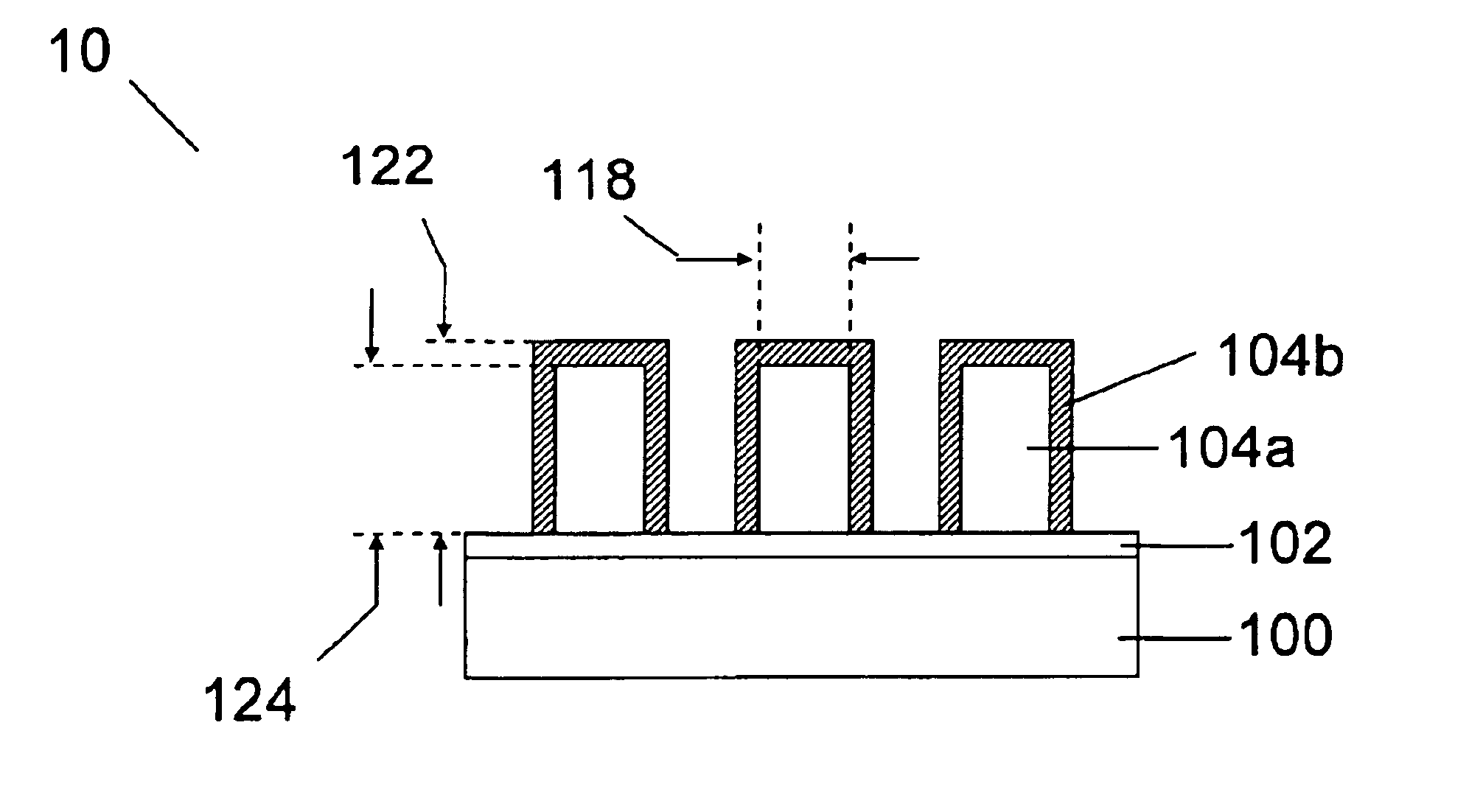
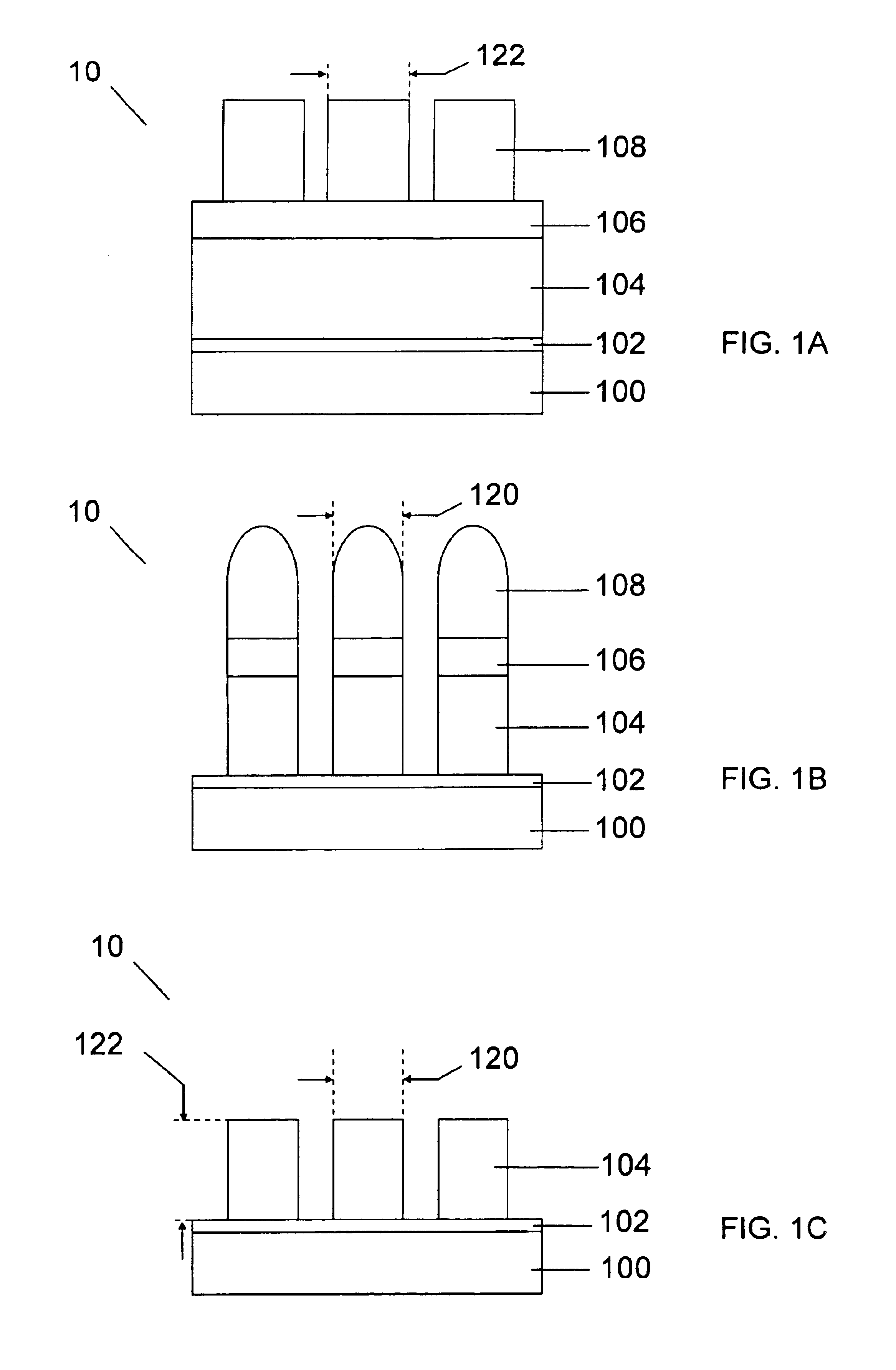
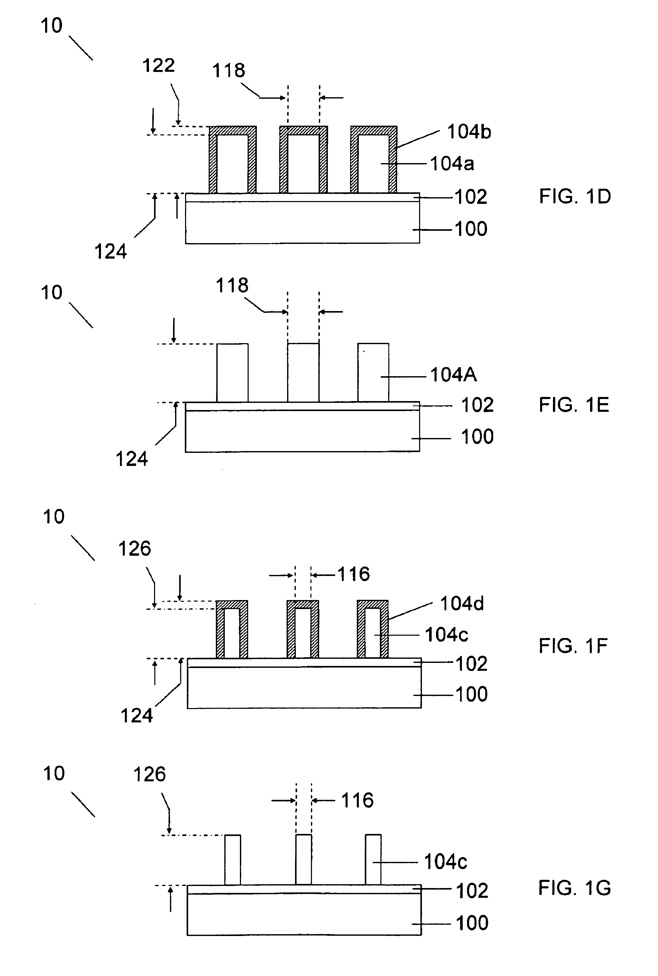
FIGS. 1A-1G show a schematic cross-sectional representation of a process flow for trimming a gate electrode structure according to an embodiment of the invention. Utilizing a soft-mask processing scheme, a dimension of a lithographically patterned gate electrode structure is trimmed by a chemical etching process. The dimension after trimming can be below the lithographic dimension of the photoresist pattern, or it can be any dimension.

FIG. 1A shows a gate electrode structure 10 containing a substrate 100, a high-k layer 102, a gate electrode layer 104, an organic ARC layer 106, and a patterned photoresist layer 108. The gate electrode layer 104 can be a Si-containing layer, e.g., amorphous Si, poly-Si, or SiGe. Alternately, the gate electrode layer 104 can be a metal-containing layer, for example a metal (e.g., Ru), a metal alloy (e.g., TiNi), a metal nitride (e.g., TaN, TaSiN, TiN, HfN), or a metal oxide (e.g., RuO2). The high-k layer 102 can, for example, contain at least one of H...


PUM


Abstract

A method and processing tool are provided for trimming a gate electrode structure containing a gate electrode layer with a first dimension. A reaction layer is formed through reaction with the gate electrode structure. The reaction layer is the selectively removed from the unreacted portion of the gate electrode structure by chemical etching, thereby forming a trimmed gate electrode structure with a second dimension that is smaller than the first dimension. The trimming process can be carried out under process conditions where formation of the reaction layer is substantially self-limiting. The trimming process can be repeated to further reduce the dimension of the gate electrode structure.

Description

FIELD OF THE INVENTIONThe present invention relates to semiconductor manufacturing, particularly to a method of reducing a dimension of a gate electrode structure using a chemical trimming process.BACKGROUND OF THE INVENTIONPlasma processing systems are used in the manufacture and processing of semiconductors, integrated circuits, displays, and other devices or materials. Plasma processing can be used to transfer a pattern of an integrated circuit from a lithographic mask to a semiconductor substrate. The lithographic mask can comprise an etch-resistant photoresist layer that is deposited over a substrate, exposed to a selected lithographic pattern and developed. In addition to the photoresist layer, the lithographic mask structure can include additional mask layers, e.g., anti-reflective coatings (ARCs). ARC layers are frequently used to reduce light reflections from the substrate during lithography steps, and sacrificial masks can be used to pattern areas on a substrate. The subst...

Claims


Application Information

Patent Timeline
IPC IPC(8): H01L21/02H01L21/28H01L21/3213
CPCH01L21/28123H01L21/32137H01L21/32136H01L21/32134
Inventor CHEN, LEEYUE, HONGYUKAMBARA, HIROMITSU
Owner TOKYO ELECTRON LTD
Why Eureka
Try Eureka