

Fabrication of low power CMOS device with high reliability
- Summary
- Abstract
- Description
- Claims
- Application Information
AI Technical Summary
Benefits of technology
Problems solved by technology
Method used
Image

Examples
Embodiment Construction
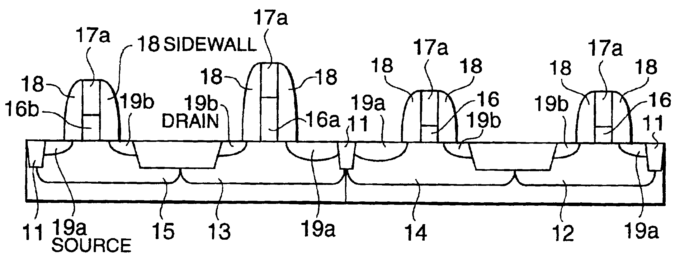
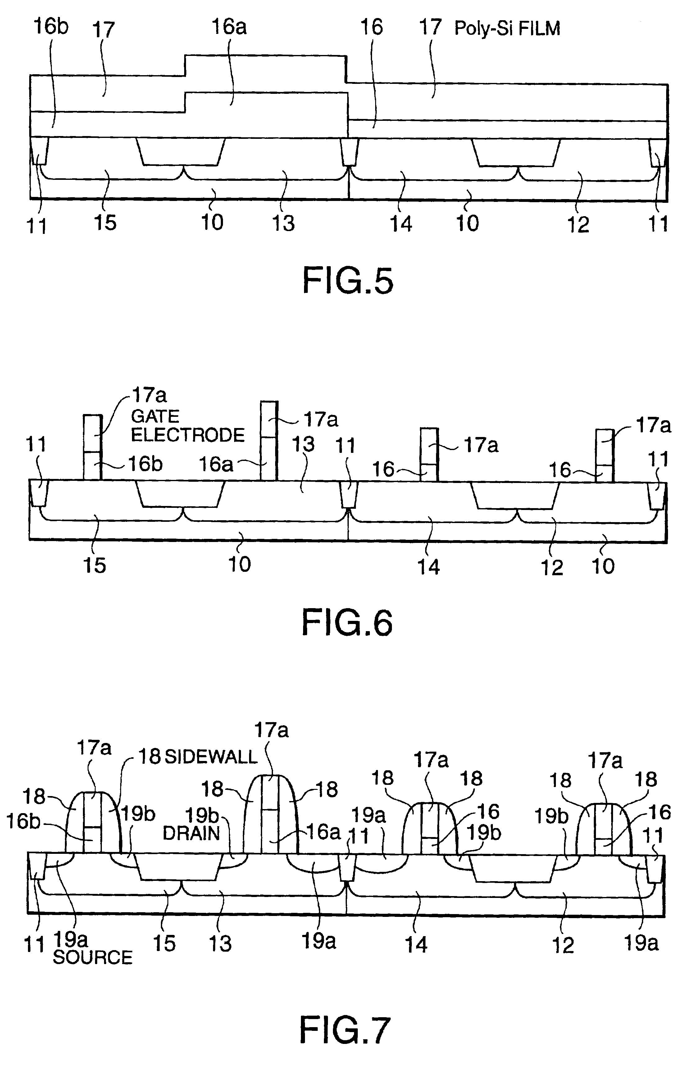
A semiconductor device according to a preferred embodiment of the present invention comprises two CMOS circuits, one of which has higher threshold MOSFETs of n- and p-types, while the other has lower threshold MOSFETs of n- and p-types. The lower threshold MOSFETs have a first gate oxide film common thereto. The higher threshold n-MOSFET has a second gate oxide film thicker than the first gate oxide film. The higher threshold p-MOSFET has a third gate oxide film which is thicker than the first gate oxide film and is thinner than the second gate oxide film.
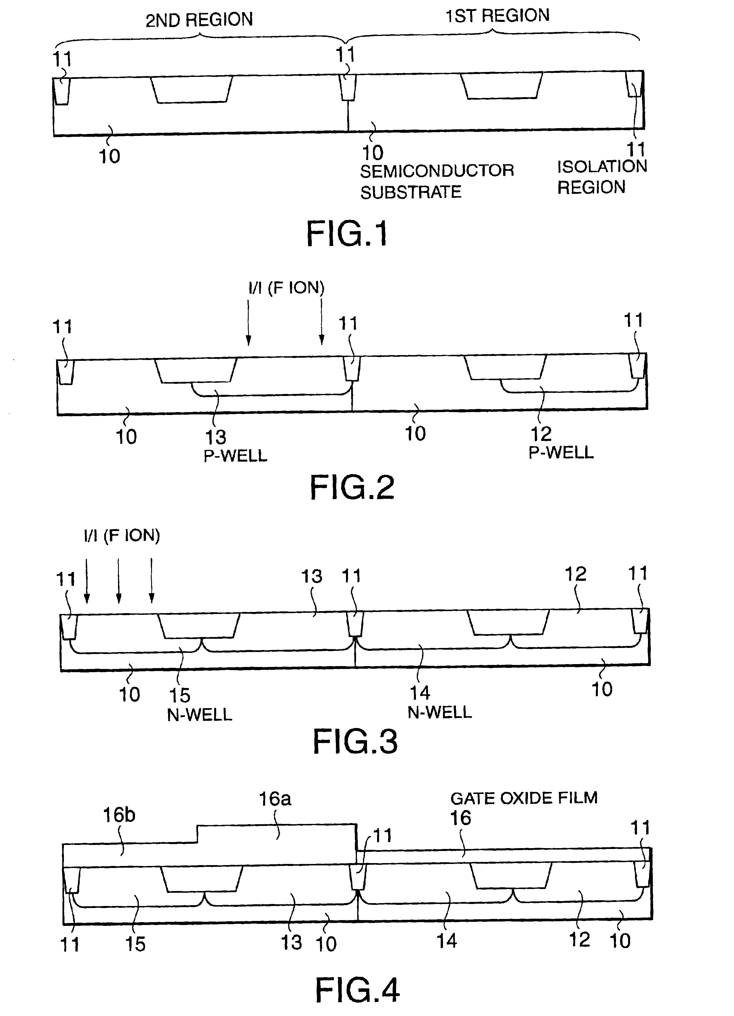
The semiconductor device can be fabricated according to the following fabrication process of the preferred embodiment of the present invention.
Referring to FIG. 1, isolation regions 11 are formed within a semiconductor substrate 10 and close to the surface of the semiconductor substrate 10, so that a first region and a second region are defined on the semiconductor substrate 10. The first region is for the lower threshold MOSFETs, ...
PUM
 Abstract
Description
Claims
Application Information