Solid state image pickup element and camera system

Inactive Publication Date: 2009-07-23
SONY CORP
View PDF2 Cites 18 Cited by
  • Summary
  • Abstract
  • Description
  • Claims
  • Application Information

AI Technical Summary

Benefits of technology

[0064]According to the present invention, a constant current can be su

Problems solved by technology

This is because the CMOS image sensor overcomes various issues of CCD, including the necessity for dedicated processes for manufacturing CCD pixels and for a plurality of power source voltages for the operation, and a very complicated sy

Method used


Image

  • Solid state image pickup element and camera system
  • Solid state image pickup element and camera system
  • Solid state image pickup element and camera system

Examples


Embodiment Construction

[0077]Embodiments of the present invention will now be described in connection with the accompanying drawings.

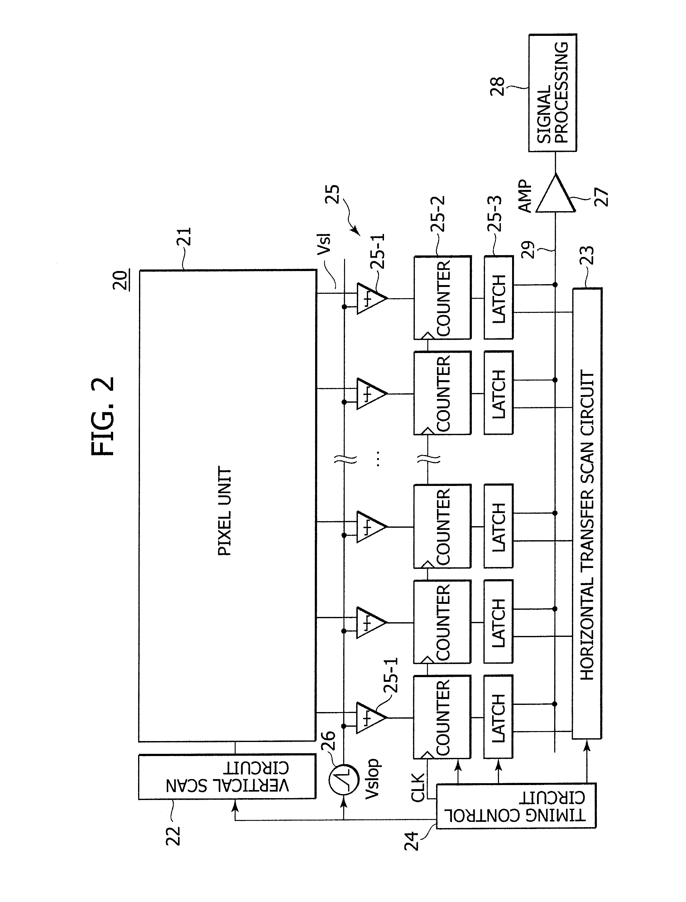
[0078]FIG. 3 is a block diagram showing an example of the structure of a column parallel ADC mounting solid state image pickup element (CMOS image sensor) according to an embodiment of the present invention.

[0079]FIG. 4 is a block diagram showing more specifically an ADC group of the column parallel ADC mounting solid state image pickup element (CMOS image sensor) shown in FIG. 3.

[0080]As shown in FIGS. 3 and 4, a solid state image pickup element 100 has a pixel unit 110 as an imaging unit, a vertical scan circuit 120, a horizontal transfer scan circuit 130, a timing control circuit 140, an ADC group 150 as a pixel signal read circuit, a DAC and bias circuit 160 including a DAC (digital-analog converter) 161, an amplifier circuit (S / A) 170, a signal processing circuit 180 and a line memory 190.

[0081]Of these constituent components, analog circuits are used for the pixel unit...


PUM


Abstract

A solid state image pickup element includes a pixel unit having a plurality of pixels for photoelectric conversion disposed in a matrix shape and a pixel signal read circuit for reading pixel signals in the unit of a plurality of pixels from the pixel unit. The pixel signal read circuit includes a plurality of comparators disposed in correspondence with a pixel column layout for performing comparison judgment between a read signal potential and a reference voltage and outputting a judgment signal and a plurality of counters each for counting a comparison time of a corresponding one of the comparators, an operation being controlled by an output from a corresponding one of the comparators. The comparators include a first amplifier for performing a comparison operation between the reference voltage and the read signal potential and inverting an output at a predetermined comparison point, a second amplifier for forming a current path when an output of the first amplifier is inverted, to output an output of the first amplifier by gain up, and a current control circuit for shutting the current path of the second amplifier when an output level of the second amplifier exceeds a predetermined threshold level.

Description

BACKGROUND OF THE INVENTION [0001]1. Field of the Invention[0002]The present invention relates to a solid state image pickup device represented by a CMOS image sensor and a camera system.[0003]2. Description of Related Art[0004]A CMOS image sensor has been paid attention as a solid state image pickup device (image sensor) to be substituted for CCD.[0005]This is because the CMOS image sensor overcomes various issues of CCD, including the necessity for dedicated processes for manufacturing CCD pixels and for a plurality of power source voltages for the operation, and a very complicated system because a plurality of peripheral IC's are required to be combined for the operation.[0006]A CMOS image sensor has a plurality of large merits: manufacturing processes similar to those for a general CMOS type integrated circuit can be used for manufacturing CMOS image sensors, a single power source can drive a CMOS image sensor, and the number of peripheral IC's can be reduced because analog circ...

Claims


Application Information

Patent Timeline
IPC IPC(8): H01L27/00H03F3/08H04N5/232H04N5/335H04N5/369H04N5/374H04N5/3745H04N5/378
CPCH04N5/378H04N5/3742H04N25/767H04N25/75
Inventor KAWAGUCHI, TAKASHITANAKA, KENICHI
Owner SONY CORP
Why Eureka
Try Eureka