This helps you quickly interpret patents by identifying the three key elements:
Problems solved by technology
Method used
Benefits of technology
Benefits of technology
[0022] Therefore, an object of the present invention is to obtain an organic EL element which is capable of converting triplet excitation energy into light to be emitted by devising a structure of a light emitting layer with using a light emitting material used in a conventional organic EL element. Thus, an object of the present invention is to provide an organic EL element which has high light emission efficiency, indicates various light emission colors by using a conventional organic compound, and can be manufactured at a low cost.
[0023] Also, an object of the present invention is to provide a light emitting device at a low cost, which is light, has low consumption power, and indicates various light emission colors, using an organic EL element disclosed by the present invention. Further, an object of the present invention is to provide an electronic device which is light, has low consumption power, indicates various light emission colors, and which has a low cost by using such a light emitting device.
Problems solved by technology
Further, since the organic EL element is a carrier injection type light emitting element, it can be driven by a direct currentvoltage and a noise is hard to cause.
However, since both platinum and iridium are so-called noble metal, the platinum complex and the iridium complex using these metals are expensive and thus it is expected that a cost reduction is hindered in future.
However, a clear molecular design plan is not established until now and is very difficult in many aspects.
Method used
Image
Click on the blue label to locate the original text in one second.
Reading with bidirectional positioning of images and text.
Examples
embodiment 1
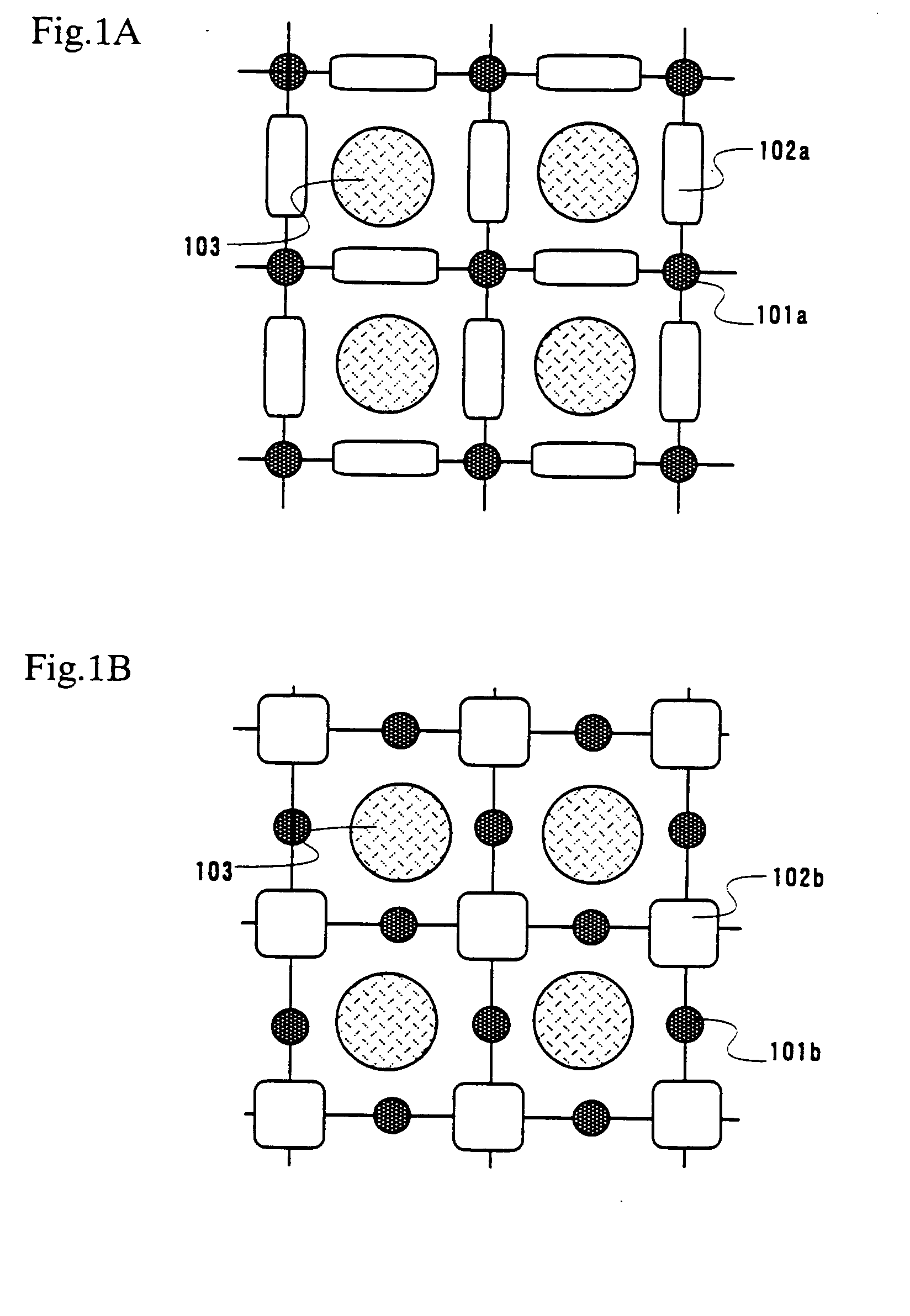
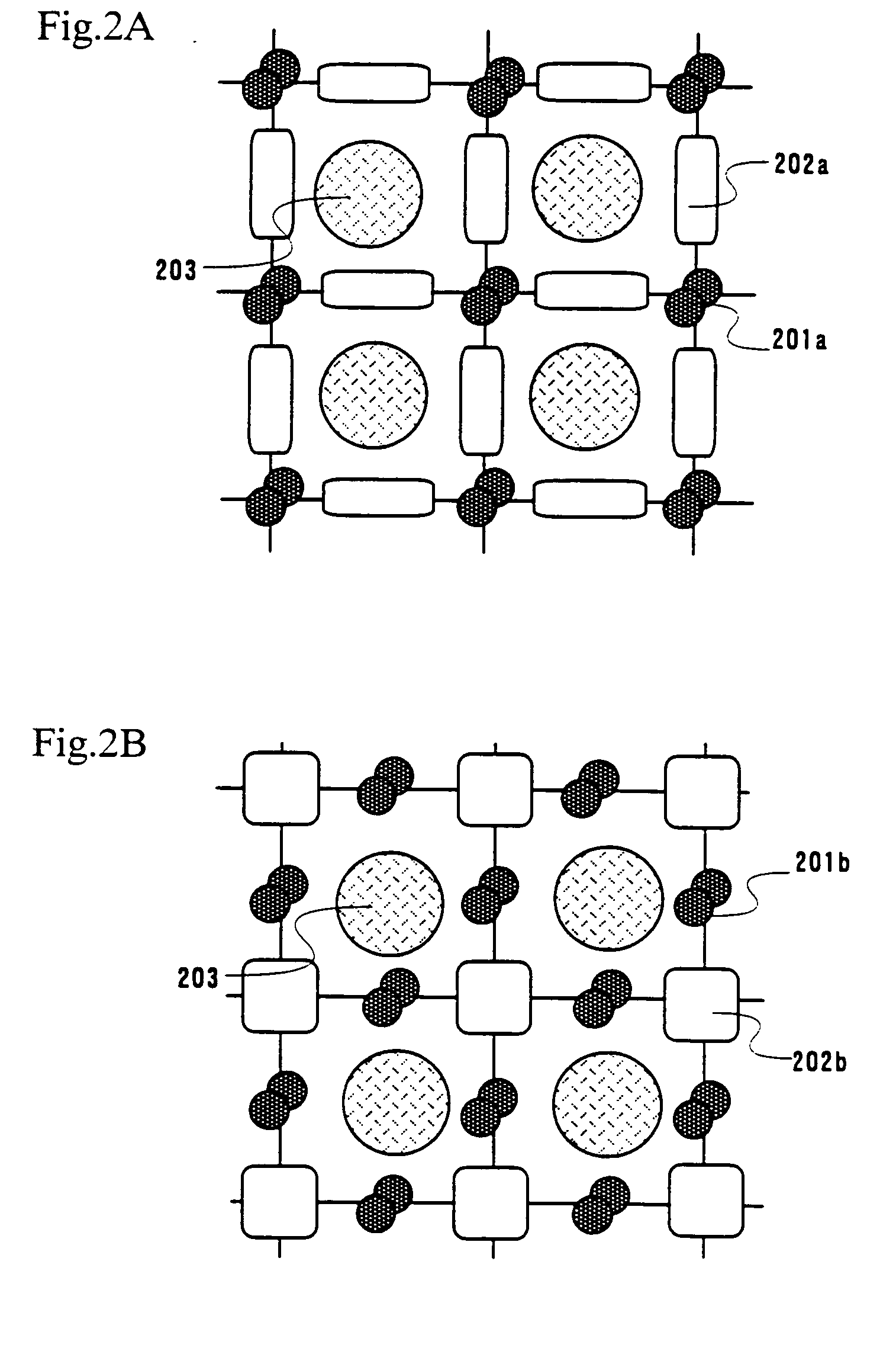
[0098] In this embodiment, an organic EL element using the metal complex as shown in FIG. 3B in the embodiment mode of the present invention will be specifically shown b an example. Cu (II) which is divalent and in which plane coordination is allowed is used as the central metal M and a compound represented by the following formula (10) is used as the ligand X.
[0100] First, an aqueous solution of polyethylenedioxythiophene (hereinafter referred to as “PEDOT”), which is doped with sulfonic acid to improve conductivity, is formed by spin coating on a glass substrate 1201 on which ITO which is a transparent anode 1202 is formed, and moisture is evaporated to produce a hole injection layer 1203. Its film thickness is desirably about 30 nm.
[0101] Then, a metal complex 1204a with a square lattice structure, made of Cu (II) which is the cental metal M and a ligand represented by the above formula (10) as the ligand X, and a light emitting material 1204b, made ...
embodiment 2
[0104] In this embodiment, an organic EL element using the metal complex as shown in FIG. 5B in the embodiment mode of the present invention will be specifically shown by an example. Ni (II) which is divalent and in which plane coordination is allowed is used as the central metal M, and a compound represented by the following formula (11) is used as the ligand X.
[0107] Then, a metal complex 1204a with a cristobalite type lattice structure, made of Ni(II) which is the cental metal M and a ligand represented by the above formula (11) as the ligand X, and a light emitting material 1204b made of Alq3 are dissolved into the same organic solvent. Thi...
embodiment 3
[0110] In this embodiment, an organic EL element using the metal complex as shown in FIG. 7 in the embodiment mode of the present invention will be specifically shown by, an example. Co(II) which is divalent and in which octahedral coordination is allowed is used as the central metal M, a compound represented by the following formula (12) is used as the ligand X, and pyrazine is used as the ligand Z.
[0113] Then, a metal complex 1204a with a hexagonal lattice structure, made of Co(II) which is the cental metal M, a ligand represented by the above formula (12) as the ligand X, and pyrazine which is the ligand Z, and a light emitting materi...
PUM
Property
Measurement
Unit
Lattice constant
aaaaa
aaaaa
Color
aaaaa
aaaaa
Structure
aaaaa
aaaaa
Abstract
There are provided a light emitting device and an electronic device, which are light, have low consumption power and a low cost. When an organic light emitting material (1204b) is included in the positions between the lattices of a heavy metal complex (1204a) with a lattice structure, the phosphorescence of the organic light emitting material (1204b) in which only fluorescence is generally observed can be promoted. Since the organic EL element obtained thus can utilize phosphorescence, the light emission efficiency is high. Also since a conventional organic light emitting material can be used, various light emission colors are obtained and the organic EL element can be manufactured at a low cost. A light emitting device and an electronic device are manufactured using such an organic EL element.
Description
BACKGROUND OF THE INVENTION [0001] 1. Field of the Invention [0002] The present invention relates to a light emitting device using an element (hereinafter referred to as “an organic EL element”) which has an anode layer, a cathode layer, and a film (hereinafter referred to as “an organic EL layer”) including an organic compound in which an EL (electro luminescence: luminescence produced by applying an electric field) is produced. As the EL in the organic compound, there are light emission (fluorescence) generated in returning from a singlet excitation state to a ground state and light emission (phosphorescence) generated in returning from a triplet excitation state to a ground state. The present invention particularly relates to a light emitting device in which a metal complex, which is capable of forming pores due to a two dimensional or a three dimensional mesh structure, is applied to a light emitting layer and thus light emitting materials are arranged in the pores to promote li...
Claims
Application Information
Patent Timeline
Application Date:The date an application was filed.
Publication Date:The date a patent or application was officially published.
First Publication Date:The earliest publication date of a patent with the same application number.
Issue Date:Publication date of the patent grant document.
PCT Entry Date:The Entry date of PCT National Phase.
Estimated Expiry Date:The statutory expiry date of a patent right according to the Patent Law, and it is the longest term of protection that the patent right can achieve without the termination of the patent right due to other reasons(Term extension factor has been taken into account ).
Invalid Date:Actual expiry date is based on effective date or publication date of legal transaction data of invalid patent.

