Method of manufacturing a magnetoresistive random access memory device and method of manufacturing a semiconductor chip including the same

Active Publication Date: 2018-11-29
SAMSUNG ELECTRONICS CO LTD
View PDF1 Cites 7 Cited by
  • Summary
  • Abstract
  • Description
  • Claims
  • Application Information

AI Technical Summary

Benefits of technology

[0007]The MRAM device in accordance with example embodiments may be fabricated to have different characteristics in different regi

Problems solved by technology

It is difficult to develop an MRAM device including the low consumption power a

Method used


Image

  • Method of manufacturing a magnetoresistive random access memory device and method of manufacturing a semiconductor chip including the same
  • Method of manufacturing a magnetoresistive random access memory device and method of manufacturing a semiconductor chip including the same
  • Method of manufacturing a magnetoresistive random access memory device and method of manufacturing a semiconductor chip including the same

Examples


Example

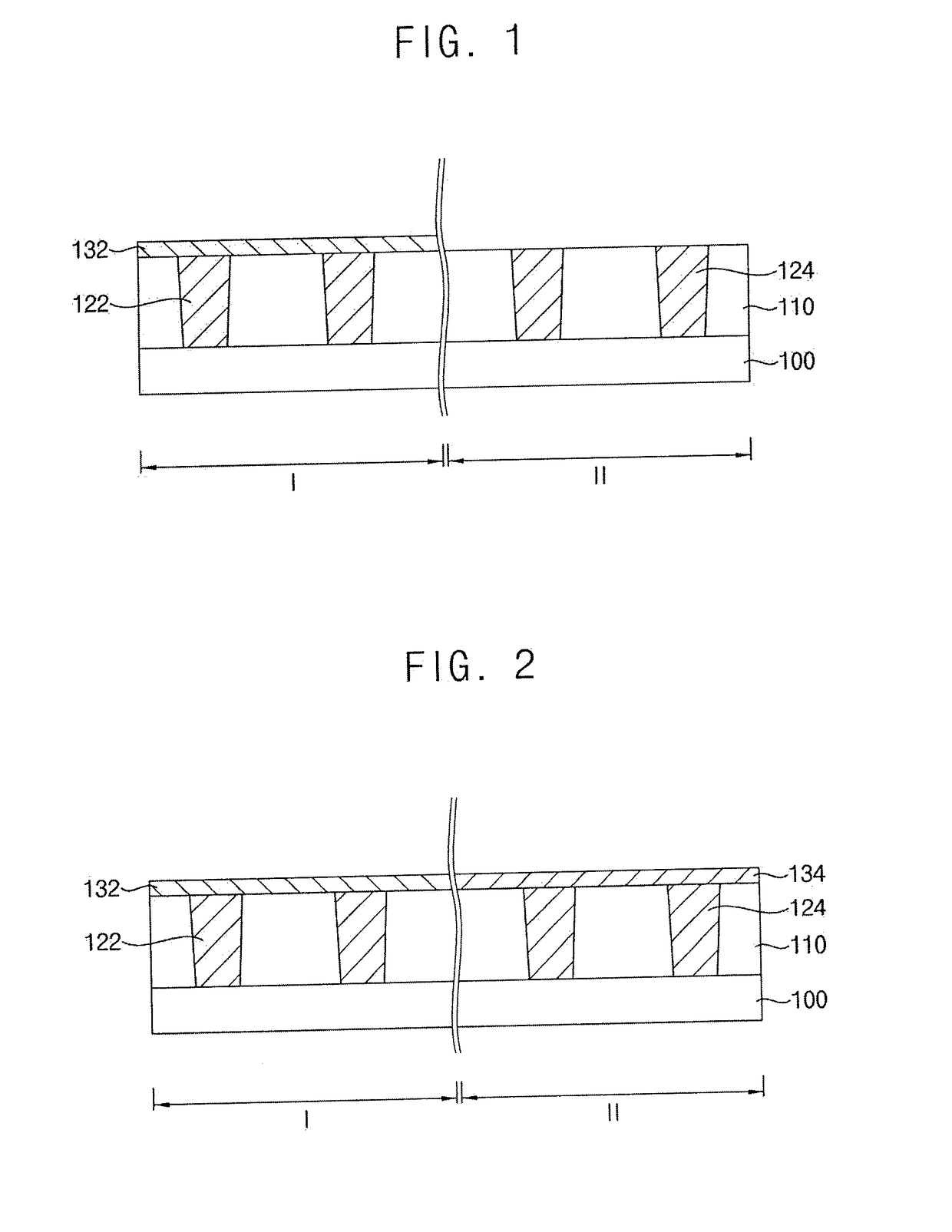
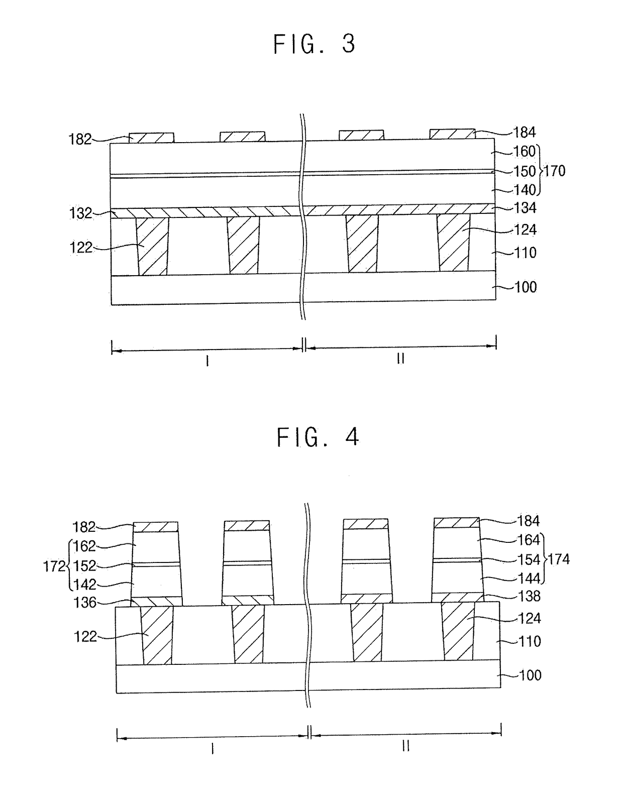
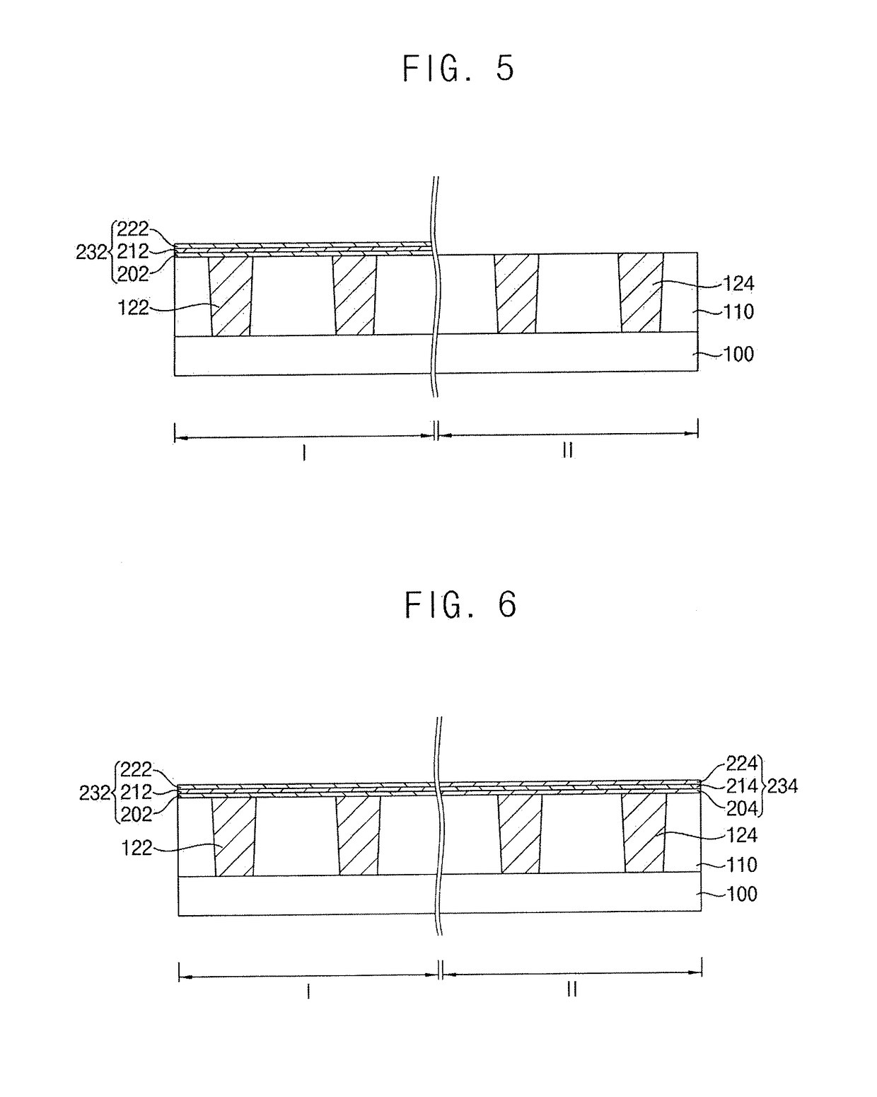
[0016]FIGS. 1 to 4 are cross-sectional views illustrating a method of manufacturing an MRAM device in accordance with example embodiments.

[0017]Referring to FIG. 1, an insulating interlayer 110 may be formed on a substrate 100, and first and second contact plugs 122 and 124 may be formed through the insulating interlayer 110.

[0018]The substrate 100 may include a semiconductor material, e.g., silicon, germanium, silicon-germanium, or III-V semiconductor compounds, e.g., GaP, GaAs, GaSb, etc. In an example embodiment, the substrate 100 may be a silicon-on-insulator (SOI) substrate or a germanium-on-insulator (GOI) substrate.

[0019]The substrate 100 may include first and second regions I and II. In example embodiments, each of the first and second regions I and II may serve as a memory cell region in which memory cells may be formed, and the first and second regions I and II may be distinguished from each other. For example, the first and second regions I and II may be spaced apart from...


PUM


Abstract

In a method of manufacturing an MRAM device, first and second lower electrodes may be formed on first and second regions, respectively, of a substrate. First and second MTJ structures having different switching current densities from each other may be formed on the first and second lower electrodes, respectively. First and second upper electrodes may be formed on the first and second MTJ structures, respectively.

Description

CROSS-REFERENCE TO RELATED APPLICATION[0001]This application claims priority under 35 USC § 119 to Korean Patent Application No. 10-2017-0065113, filed on May 26, 2017 in the Korean Intellectual Property Office (KIPO), the contents of which are herein incorporated by reference in their entirety.BACKGROUND1. Technical Field[0002]Example embodiments relate to methods of manufacturing a semiconductor device and methods of manufacturing a semiconductor chip including the same. More particularly, example embodiments relate to methods of manufacturing a magnetoresistive random access memory (MRAM) device and methods of manufacturing a semiconductor chip including the same.2. Description of Related Art[0003]If a switching current density for changing the magnetization direction of a free layer of an MTJ is low, an MRAM device including the MTJ may have a low consumption power and a high operation speed. However, if the switching current density is high, the MRAM device may have a high data...

Claims


Application Information

Patent Timeline
IPC IPC(8): H01L43/12H01L43/08H01L43/02H01L27/22G11C11/16
CPCH01L43/12H01L43/08H01L43/02H01L27/228G11C11/161H01L21/77H10B61/00H10N50/01H10N50/10H01L29/41791H10B61/22H10N50/80
Inventor KIM, DAE-SHIKPARK, JEONG-HEONKOH, GWAN-HYEOB
Owner SAMSUNG ELECTRONICS CO LTD
Why Eureka
Try Eureka