Resistance random access memory and method of manufacturing the same

a random access memory and resistance technology, applied in the direction of basic electric elements, electrical equipment, semiconductor devices, etc., can solve the problems of low degree of integration and operating speed of drams, inability to easily perform etching processes, and loss of all data stored in drams, so as to reduce the manufacturing cost of memory, improve the electrical characteristics, and be flexible

Active Publication Date: 2008-07-10
SAMSUNG ELECTRONICS CO LTD
View PDF8 Cites 37 Cited by
  • Summary
  • Abstract
  • Description
  • Claims
  • Application Information

AI Technical Summary

Benefits of technology

[0015]Example embodiments provide a resistance random access memory (RRAM) including a resistance layer, which may be formed using a lower temperature deposition and which ma

Problems solved by technology

However, when the power supply to the DRAM is discontinued, all data stored in the DRAM is lost.
However, although flash memory devices have nonvolatile characteristics unlike a volatile memory device, the degree of integration and operating speed thereof is less than those of a DRAM.
In a PRAM manufacturing process, an etching process cannot ea

Method used


Image

  • Resistance random access memory and method of manufacturing the same
  • Resistance random access memory and method of manufacturing the same
  • Resistance random access memory and method of manufacturing the same

Examples


example 1

RRAM Including a NiO Layer Having 0.05 wt % of a Ti Ion

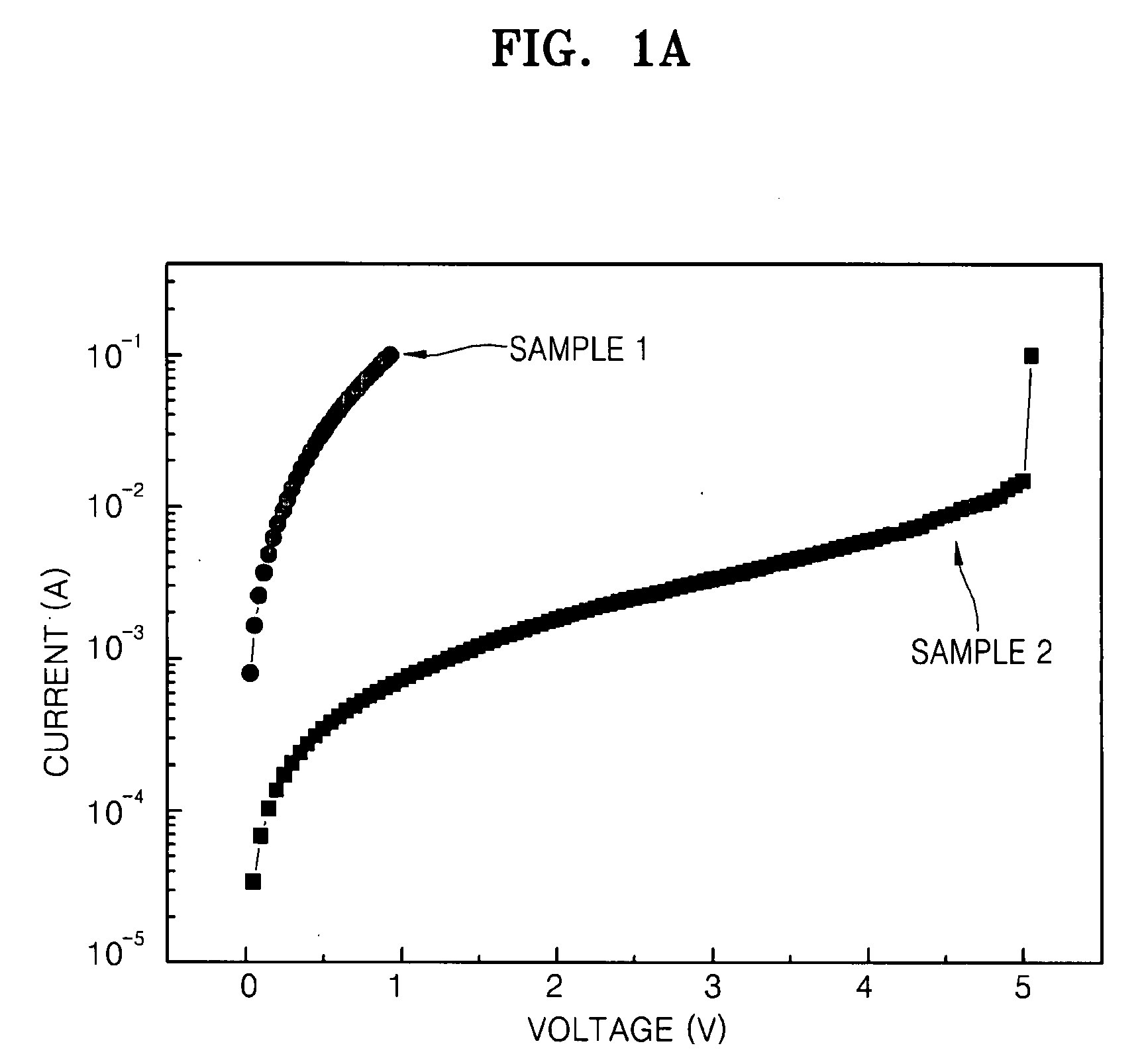
[0056]A Pt electrode was formed on a substrate with a thickness of 50 nm. A NiO layer with a thickness of 500 Å and a size of 100 μm×100 μm having 0.05 wt % of a Ti ion was formed on the Pt electrode using a reactive sputtering method using a Ni target doped with 0.05 wt % of the Ti ion (O2 partial pressure: 10 mol %, temperature during the sputtering: room temperature of about 25° C.). Then, a Pt electrode was formed on the NiO layer having 0.05 wt % of the Ti ion to prepare an RRAM.

example 2

RRAM Including a NiO Layer Having 0.1 wt % of a Ti Ion

[0057]A RRAM was manufactured in the same manner as in Example 1 except that a NiO layer having 0.1 wt % of a Ti ion was formed using a Ni target doped with 0.1 wt % of the Ti ion instead of the Ni target doped with 0.05 wt % of the Ti ion.


PUM


Abstract

Provided are a resistance random access memory including a resistance layer having a metal oxide and/or a metal ion dopant, which may be deposited at room temperature and which may have variable resistance characteristics, and a method of manufacturing the same.

Description

PRIORITY STATEMENT[0001]This application claims priority under 35 USC § 119 to Korean Patent Application No. 2007-0001160, filed on Jan. 4, 2007, in the Korean Intellectual Property Office (KIPO), the entire contents of which are herein incorporated by reference.BACKGROUND[0002]1. Field[0003]Example embodiments relate to a resistance random access memory (RRAM) including a resistance layer having a metal oxide and / or a metal ion dopant and a method of manufacturing the same. The resistance layer of the RRAM may be formed at a lower temperature and may have better electrical characteristics, and thus an RRAM including the resistance layer may be more reliable and may be manufactured in a more cost-effective manner.[0004]2. Description of Related Art[0005]A semiconductor memory array includes many memory cells connected in a circuit. In a Dynamic Random Access Memory (DRAM), which is an example of a semiconductor memory device, a unit memory cell is composed of a switch and a capacito...

Claims


Application Information

Patent Timeline
IPC IPC(8): H01L29/00H01L21/20
CPCH01L45/04H01L45/1233H01L27/2436H01L45/1625H01L45/146H10B63/30H10N70/20H10N70/826H10N70/8833H10N70/026H10B99/00
Inventor LEE, MYOUNG-JAELEE, EUN-HONGPARK, YOUNG-SOO
Owner SAMSUNG ELECTRONICS CO LTD
Why Eureka
Try Eureka