Semiconductor device and manufacturing method for the same

Inactive Publication Date: 2006-07-04
RENESAS ELECTRONICS CORP
View PDF4 Cites 20 Cited by
  • Summary
  • Abstract
  • Description
  • Claims
  • Application Information

AI Technical Summary

Benefits of technology

[0015]Therefore, the present invention provides a bipolar junction transist

Problems solved by technology

However, in existent bipolar transistors, the parasitic capacitance between

Method used


Image

  • Semiconductor device and manufacturing method for the same
  • Semiconductor device and manufacturing method for the same
  • Semiconductor device and manufacturing method for the same

Examples


Example

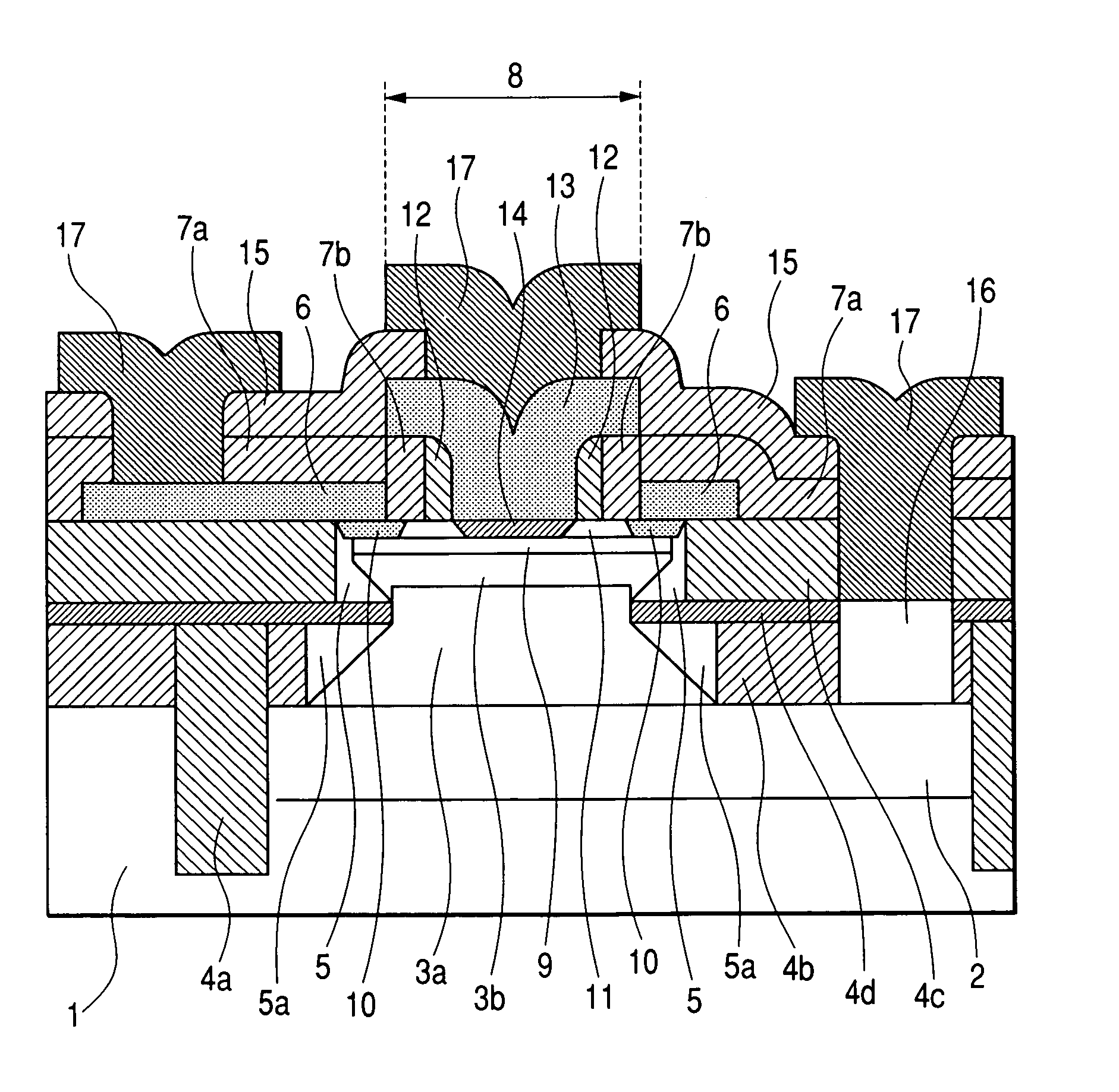
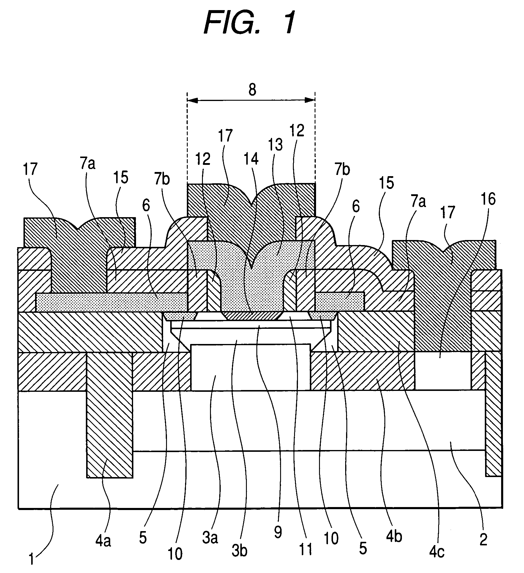
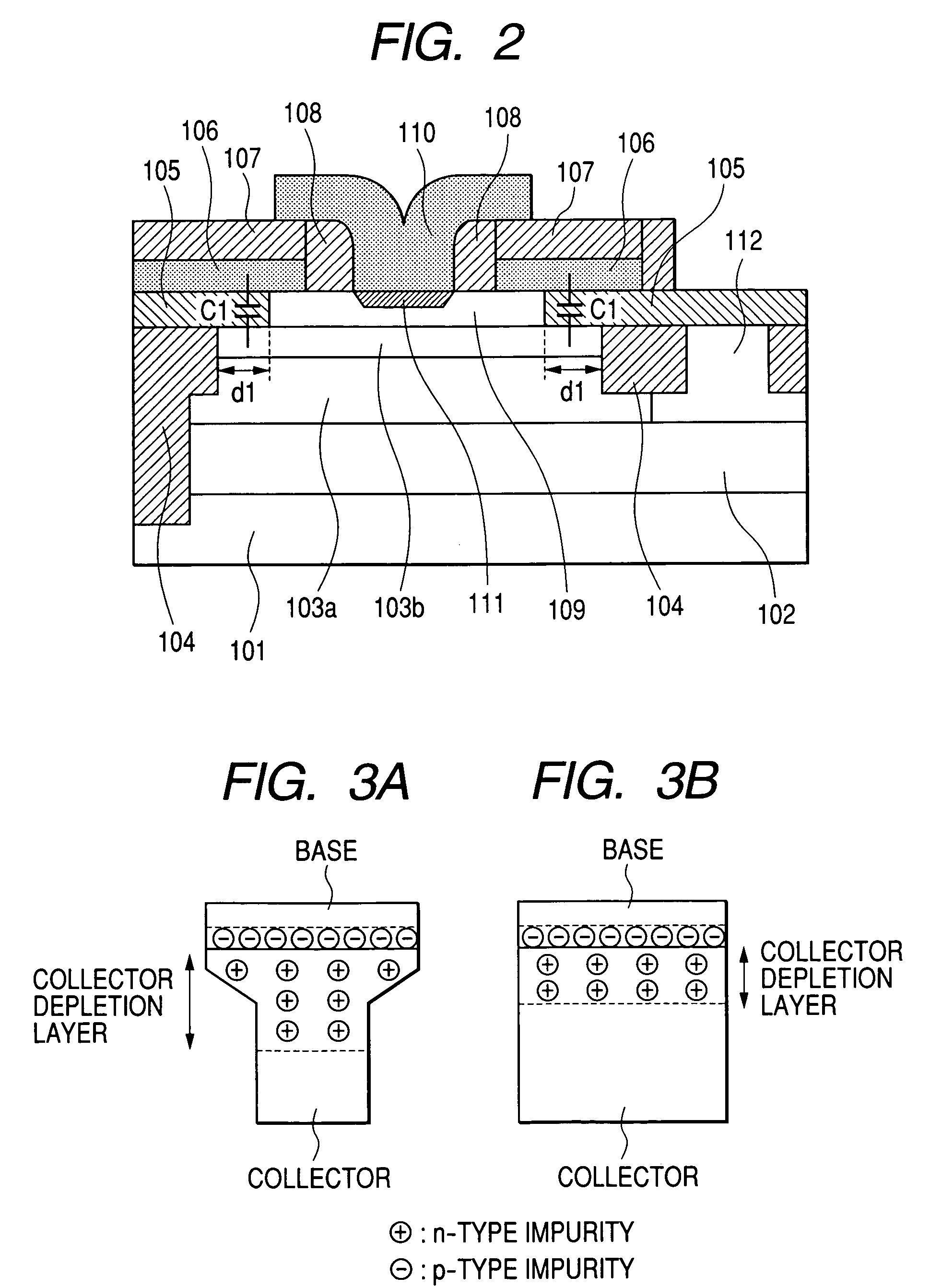
[0031]It is to be understood that the figures and descriptions of the present invention have been simplified to illustrate elements that are relevant for a clear understanding of the present invention, while eliminating, for purposes of clarity, many other elements found in a typical semiconductor device and method. Those of ordinary skill in the art will recognize that other elements are desirable and / or required in order to implement the present invention. But because such elements are well known in the art, and because they do not facilitate a better understanding of the present invention, a discussion of such elements is not provided herein. The disclosure herein is directed to all such variations and modifications to the applications, networks, systems and methods disclosed herein and as will be known, or apparent, to those skilled in the art.

[0032]In the present invention, a collector layer of single or plural layers may be disposed on a silicon substrate, the side wall for th...


PUM


Abstract

A bipolar semiconductor device including a collector layer covered at a portion of an outer periphery thereof with an insulating film and having a shape extending in an upper direction and a horizontal direction, with a gap being formed between the collector layer and the insulating film, and further including a base layer and an emitter layer disposed over the collector layer, and a manufacturing method of the semiconductor device. Since the collector layer has a shape extending in a portion thereof in the upward direction and the horizontal direction, an external collector region can be deleted, and both the parasitic capacitance and the collector capacitance in the intrinsic portion attributable to the collector can be decreased and, accordingly, a bipolar transistor capable of high speed operation at a reduced consumption power can be constituted.

Description

CLAIM OF PRIORITY[0001]The present application claims priority from Japanese Application JP 2003-174228 filed on Jun. 19, 2003, the content of which is hereby incorporated by reference as if set forth in the entirety herein.FIELD OF THE INVENTION[0002]The present invention relates to a semiconductor device and a manufacturing method thereof, and more particularly to a semiconductor device and method including at least one bipolar junction transistor.BACKGROUND OF THE INVENTION[0003]In recent years, bipolar transistors having high speed performance have been used in various fields of application, such as communication devices and storage systems. A bipolar transistor capable of increasing operation speed is the bipolar transistor using a selective epitaxial technology disclosed, for example, in JP-A No. 7-147287. FIG. 2 illustrates a p-type base layer 109 and an n-type type emitter region 111 formed in a patterned structure, wherein the width of the base layer 109 is determined by th...

Claims


Application Information

Patent Timeline
IPC IPC(8): H01L31/072H01L21/331H01L29/08H01L29/417H01L29/732H01L29/737
CPCH01L29/0821H01L29/732H01L29/66287H01L29/41708
Inventor MIURA, MAKOTOWASHIO, KATSUYOSHISHIMAMOTO, HIROMI
Owner RENESAS ELECTRONICS CORP
Why Eureka
Try Eureka