Check patentability & draft patents in minutes with Patsnap Eureka AI!

Amplifier power control circuit

Inactive Publication Date: 2005-02-08
QORVO US INC
View PDF12 Cites 4 Cited by
  • Summary
  • Abstract
  • Description
  • Claims
  • Application Information

AI Technical Summary

Benefits of technology

Embodiments of the power control circuit offer several advantages, especially if formed on the same integrated circuit chip as the amplifier. In addition to being independent of the reference voltage (e.g., a power supply voltage) supplied to the chip, the power control circuit takes up only a small area on the chip. Further, cost is minimal since the power control circuit may be simultaneously fabricated with the amplifier and any associated on-chip circuits. Further, no output power is lost since the sense signal is taken from the input side of the amplifier. Such advantages are useful in, for example, cellular telephone handsets.

Problems solved by technology

Such an output power level may be required to change with time.
A disadvantage of directional couplers, however, is that some coupling loss exists as the output signal is sampled.
In addition, directional couplers are typically large, a condition which prevents the coupler from being on the same integrated circuit as the amplifier.
Furthermore, adding an off-chip coupler to an electronic device increases the cost of the device.

Method used


Image

  • Amplifier power control circuit
  • Amplifier power control circuit
  • Amplifier power control circuit

Examples


Embodiment Construction

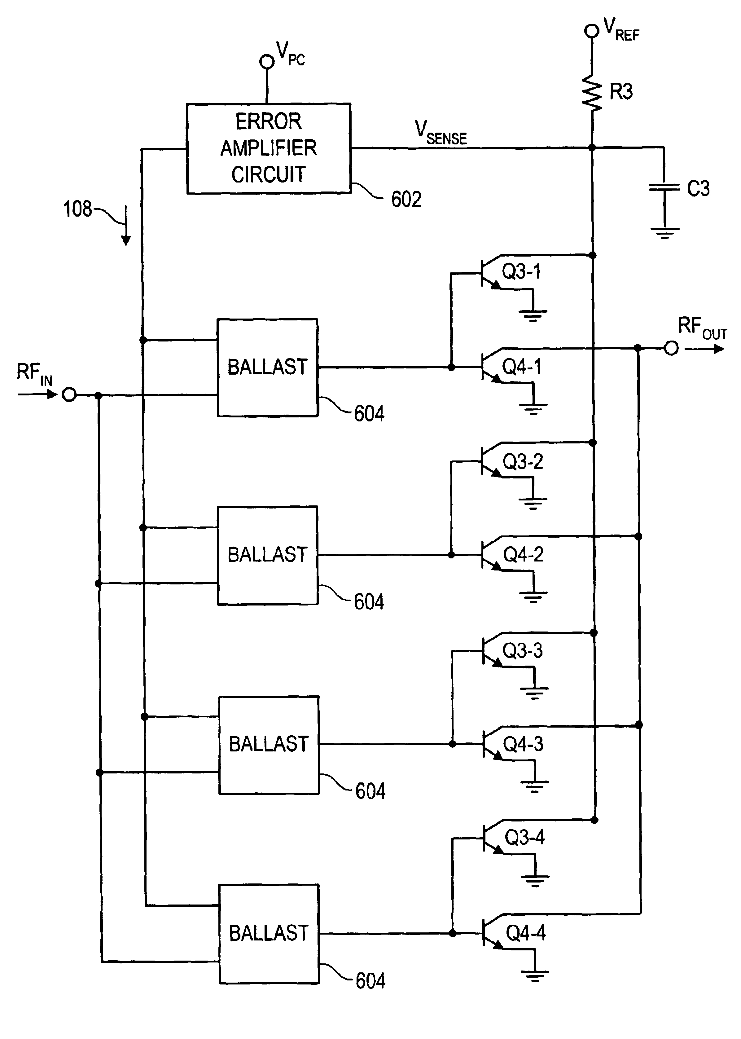
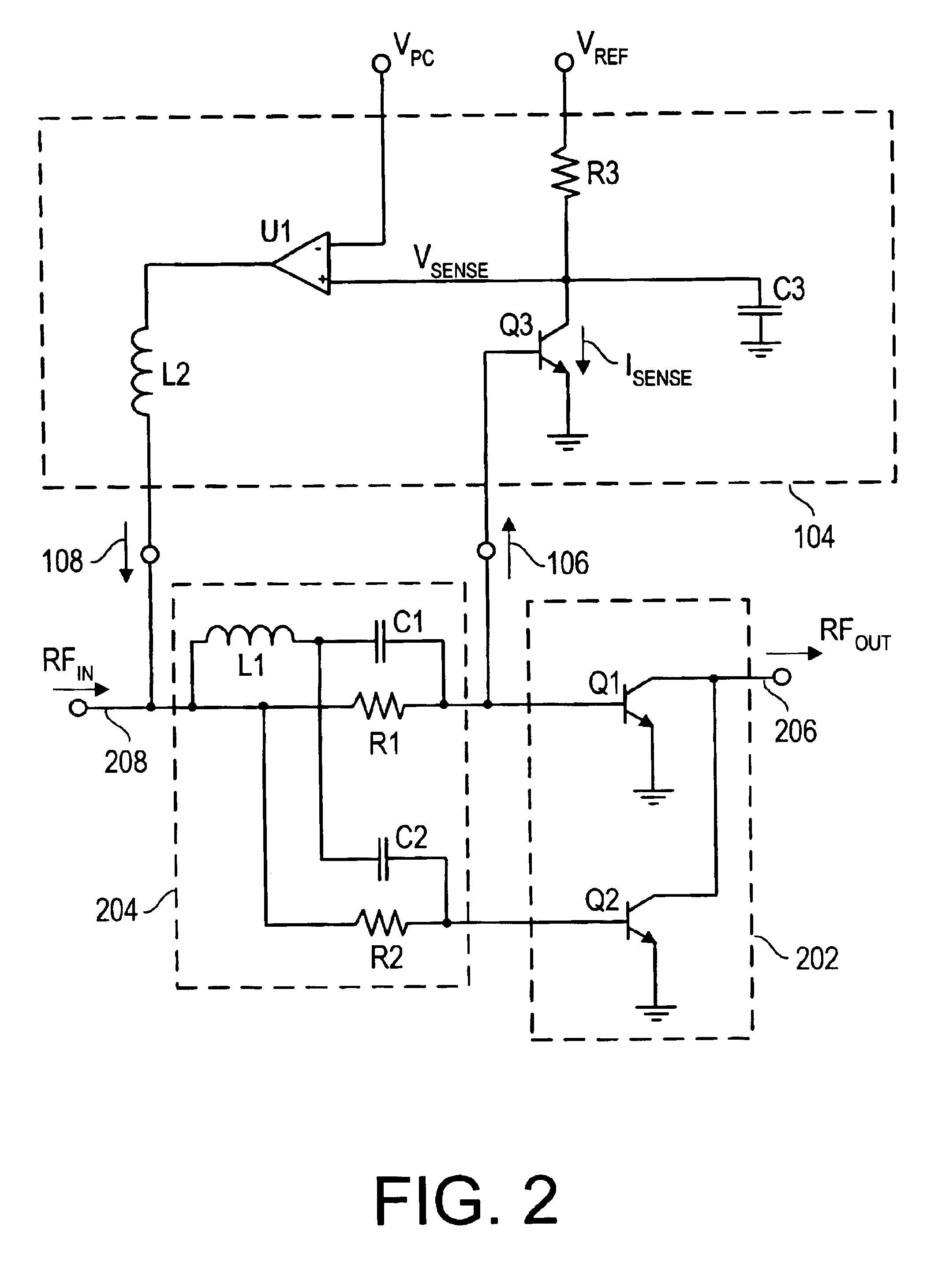
As described herein, error amplifiers are voltage amplifiers that amplify the voltage difference between a pair of inputs. Skilled individuals will be familiar with various error amplifier (operational amplifier) circuit topologies. For descriptive convenience, the error amplifier inputs are referred to as inverting (−) and non-inverting (+). Skilled individuals will understand that well-known circuit elements may have been omitted from one or more of the accompanying drawings so as to more clearly illustrate the embodiments.

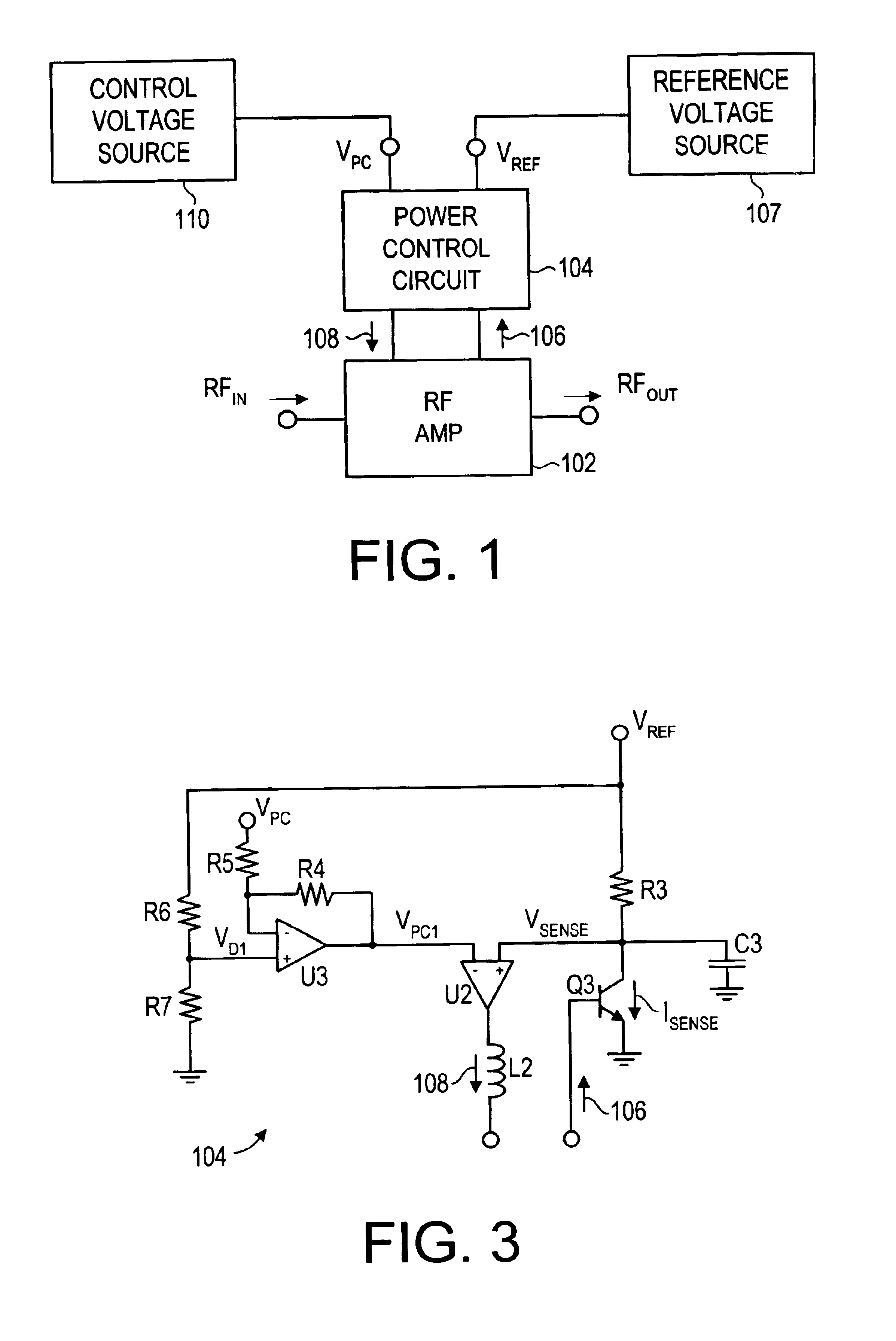
FIG. 1 is a diagrammatic view showing functional blocks in an amplifier and power control circuit combination. As shown in FIG. 1, radio frequency (RF) amplifier102 receives RF signal RFIN, which in some instances is a modulated RF carrier at about 1-2 GigaHertz, although any AC signal frequency may be used. Amplifier 102 amplifies signal RFIN and outputs signal RFOUT. In accordance with the invention, power control circuit 104 receives output power sense signal...


PUM


Abstract

A sense transistor is placed in a current path between a reference voltage source and ground. The base terminal of the sense transistor is coupled to the base terminal of an amplifying transistor. Thus, current in the sense transistor corresponds to signal power output by the amplifying transistor. The sense current causes a sense voltage at the collector terminal of the sense transistor. This sense voltage is applied to one input of an error amplifier. The other error amplifier input receives a power control voltage. The error amplifier output is routed back to the base terminal of the amplifying transistor in a negative feedback loop, thereby keeping the power of the signal output by the amplifying transistor at a constant level. In some embodiments the error amplifier output is made independent of changes in the reference voltage. Multiple pairs of corresponding amplifying and sense transistors can be used.

Description

BACKGROUND1. Field of InventionEmbodiments relate to electronic amplifier output signal power detection and control, particularly for radio frequency (RF) signals output from one or more final stage amplifying transistors.2. Related ArtMany electronic circuit applications require that output power of an amplifier be detected and controlled to maintain a specified level. Such an output power level may be required to change with time. In a Global System for Mobile communications (GSM) cellular telephone handset, for example, the final stage radio frequency (RF) amplifier outputs a signal to the antenna, and the power level of this signal must be controlled to maintain one or more precise levels. Therefore, it is important to be able to determine amplifier output power level and to control that power level.The power of a signal output from a Class C or similar transistor amplifier with non-continuous conduction corresponds to the collector current. In such amplifiers, two or more trans...

Claims


Application Information

Patent Timeline
IPC IPC(8): H03F3/189H03F3/19H03F1/30
CPCH03F1/302H03F3/19H03F2203/21178
Inventor BACHHUBER, STEPHEN P.APEL, THOMAS R.KNAPP, ROBERT E.
Owner QORVO US INC
Features
  • R&D
  • Intellectual Property
  • Life Sciences
  • Materials
  • Tech Scout
  • Unparalleled Data Quality
  • Higher Quality Content
  • 60% Fewer Hallucinations
Learn More