Plasma display panel and plasma display device

a technology of plasma display panel and display device, which is applied in the direction of static indicating device, address electrode, instruments, etc., can solve the problems of high cost, no sustain discharge, and disadvantageous lift-off method of vapor deposition, and achieve the effect of increasing the minimum sustain pulse voltag

Inactive Publication Date: 2005-02-15
MITSUBISHI ELECTRIC CORP
View PDF23 Cites 40 Cited by
  • Summary
  • Abstract
  • Description
  • Claims
  • Application Information

AI Technical Summary

Benefits of technology

It is an object of the present invention to provide a plasma display panel substrate and a PDP which can suppress a significant increase in the minimum sustain pulse voltage required for a sustain discharge.
The predetermined potential difference is supplied between adjacent first electrodes during the reset period, while extension of the surface discharge generated on the first substrate to the exposed surface of the discharge inert film is suppressed. This prevents accumulation of wall charges with probability in the discharge inert film through the priming discharge, to stabilize initialization of the wall charges after the above supply of predetermined potential difference or the above generation of surface discharge. As a result, it is possible to ensure the cell selectivity during the writing period after the reset period and surely generate the sustain discharge in the selected discharge cell during the discharge sustain period after the writing period.

Problems solved by technology

Since costly processes of photolithography, vapor deposition and lift-off are executed, however, the vapor deposition lift-off method itself disadvantageously requires high cost.
On the other hand, in the cell not selected in the writing period AD, which does not have sufficient wall charge which is needed to start the sustain discharge, no sustain discharge is generated.

Method used


Image

  • Plasma display panel and plasma display device
  • Plasma display panel and plasma display device
  • Plasma display panel and plasma display device

Examples


Embodiment Construction

The First Preferred Embodiment

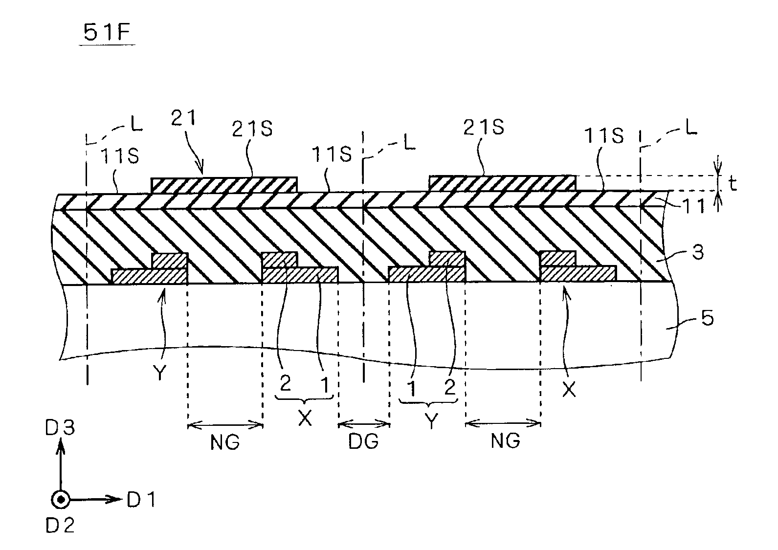
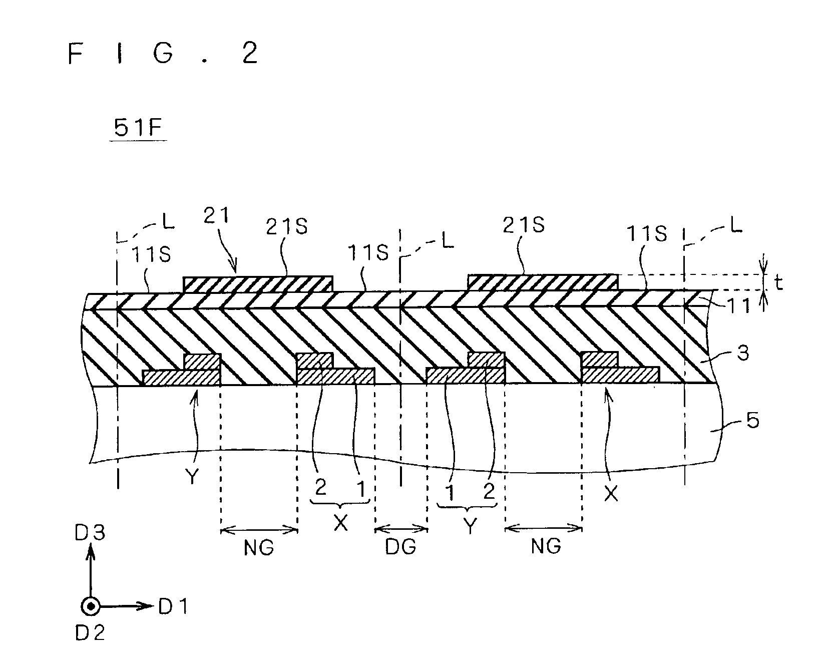
As discussed above, when the inventor of the present invention tries to form a discharge inert film, as the discharge inert film 21P of the PDP 51P, of a dielectric glass whose main material is TiO2 or Al2O3 by screen printing, with a thickness of several μm, it is found that the minimum sustain pulse voltage required for a sustain discharge between the paired sustain discharge electrodes X and Y becomes higher than usual and a practical driving is difficult.

Though detailed mechanism is uncertain since this is a phenomenon which never occurs in the discharge inert film 21P made of TiO22 or Al2O3, which is patterned by the vapor deposition lift-off method, this is thought to be caused by formation of a discharge inert film of a dielectric glass whose main material is TiO2 or Al2O3 by screen printing to have a thickness of several μm.

Then, the first preferred embodiment is intended to provide a PDP which can solve such a problem and a plasma display devic...


PUM


Abstract

A discharge inert film (22) is made of an aggregate of fine particles not substantially containing any inorganic binder. Each of sustain discharge electrodes (XB, YB) includes a plurality of discharge gap adjoining portions (a), a bus portion (b) and a plurality of bridge-building portions (c). The bus portion (b) adjoins the electrode pair gap portion (NG), extending along a second direction (D2). Each of bridge-building portions (c) extends towards a discharge gap portion (DG). The bridge-building portions (c) are connected to the discharge gap adjoining portions (a), respectively, and these adjoining portions (a) adjoin the discharge gap portion (DG) and are arranged therealong. The film (22) is so disposed as not to cover the discharge gap adjoining portions (a). When a surface discharge is generated between the sustain discharge electrodes (X, Y) during a reset period, the potential difference between the electrodes (X, Y) is gradually increased.

Description

BACKGROUND OF THE INVENTION1. Field of the InventionThe present invention relates to a plasma display panel (also referred to as “PDP”) and a plasma display device.2. Description of the Background ArtFIG. 23 is a perspective view illustrating a PDP 51P including a discharge inert film, which is disclosed in Japanese Patent Application Laid Open Gazette No. 9-102280. The discharge inert film is also reffered to as a “discharge deactivation film”, as a “discharge passivation film” or as a “discharge inhibiting film”. The PDP 51P of FIG. 23 is a surface discharge type AC-PDP. The PDP 51P is broadly divided into a front substrate 51FP, a rear (or back) substrate 51R, and a barrier rib 7 and a phosphor 8 which are disposed between the front substrate 51FP and the rear substrate 51R.The front substrate 51FP includes a front glass substrate 5, a plurality of sustain discharge electrodes X and Y, a dielectric layer 3, a cathode film 11 and a discharge inert film 21P. In more detail, a plura...

Claims


Application Information

Patent Timeline
Patent Type & Authority Patents(United States)
IPC IPC(8): H01J17/49H01J11/12H01J11/22H01J11/24H01J11/26H01J11/34H01J11/40H01J11/44
CPCH01J11/12H01J11/24H01J11/40H01J2211/323H01J2211/245
Inventor NAGANO, SHINICHIRO
Owner MITSUBISHI ELECTRIC CORP
Why Eureka
Try Eureka