Semiconductor memory device

a memory device and semiconductor technology, applied in the direction of information storage, static storage, digital storage, etc., can solve the problems of margin failure, inability to consider a procedure for evaluating margin insufficiency, and difficulty in confirming the pulse width required at the location of margin failur

Inactive Publication Date: 2005-02-15
HITACHI LTD
View PDF5 Cites 28 Cited by
  • Summary
  • Abstract
  • Description
  • Claims
  • Application Information

AI Technical Summary

Benefits of technology

[0009]It is thus an object of the present invention to present a technology capable of evaluating a margin insufficiency of the pulse width of a clock si

Problems solved by technology

Nevertheless, the technologies do not consider a procedure for evaluating a margin insufficiency of the pulse width of a clock signal and feeding back a result of the evaluation to a design phase for, among other purposes, correction of a layout on the basis of the result.
Thus, at some locations in the semiconductor memory device, it is quite within the bounds of possibility that there has been a margin failure, which can otherwise be detected by carrying out an evaluation and/or an analysis.
As another problem, it

Method used


Image

  • Semiconductor memory device
  • Semiconductor memory device
  • Semiconductor memory device

Examples


Embodiment Construction

a diagram showing another typical circuit configuration of the circuit for setting logic of a pulse-width control signal in the SRAM;

[0041]FIG. 17 is a diagram showing a further typical circuit configuration of the circuit for setting logic of a pulse-width control signal in the SRAM;

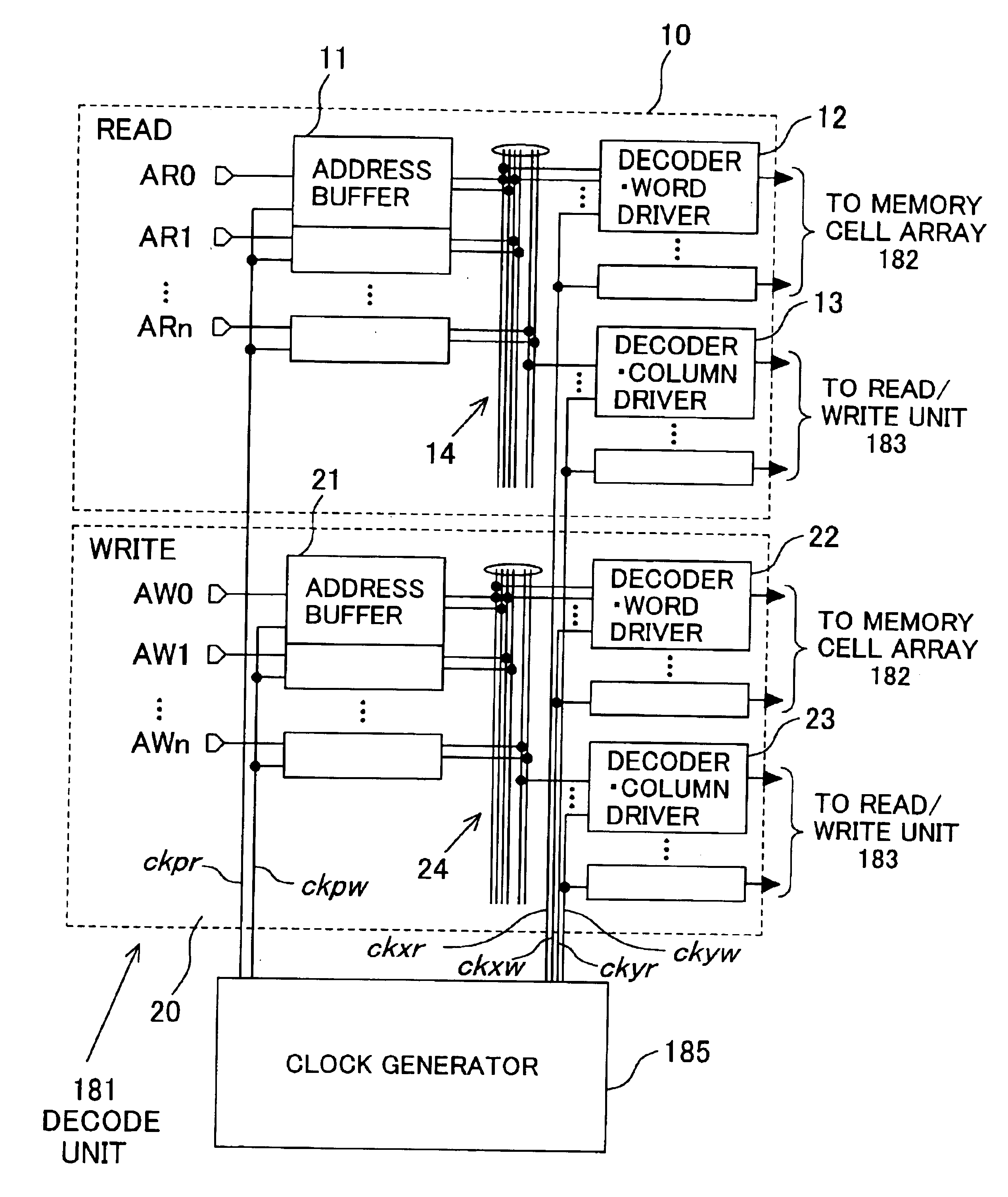
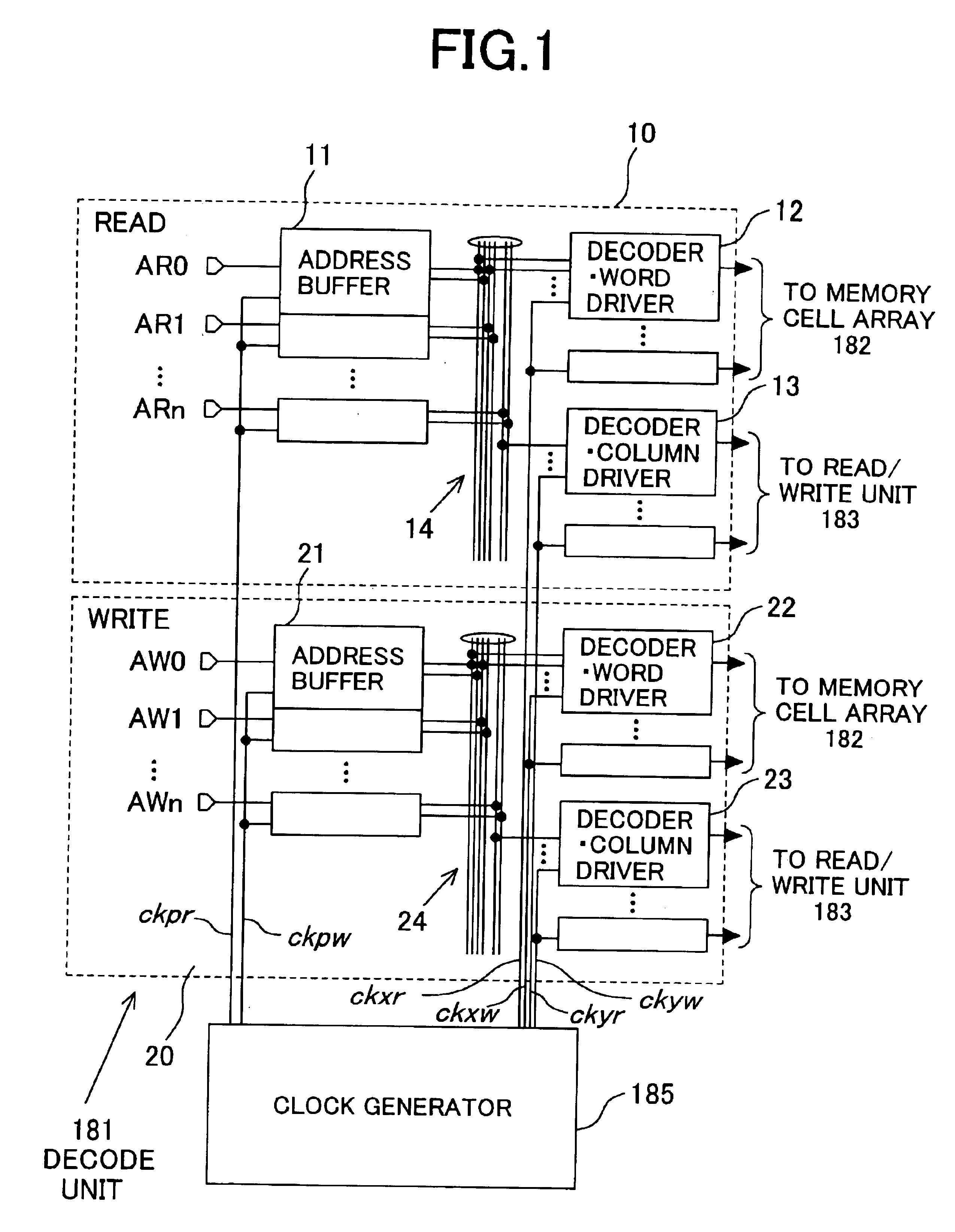
[0042]FIG. 18 is a block diagram showing an overall configuration of the SRAM;

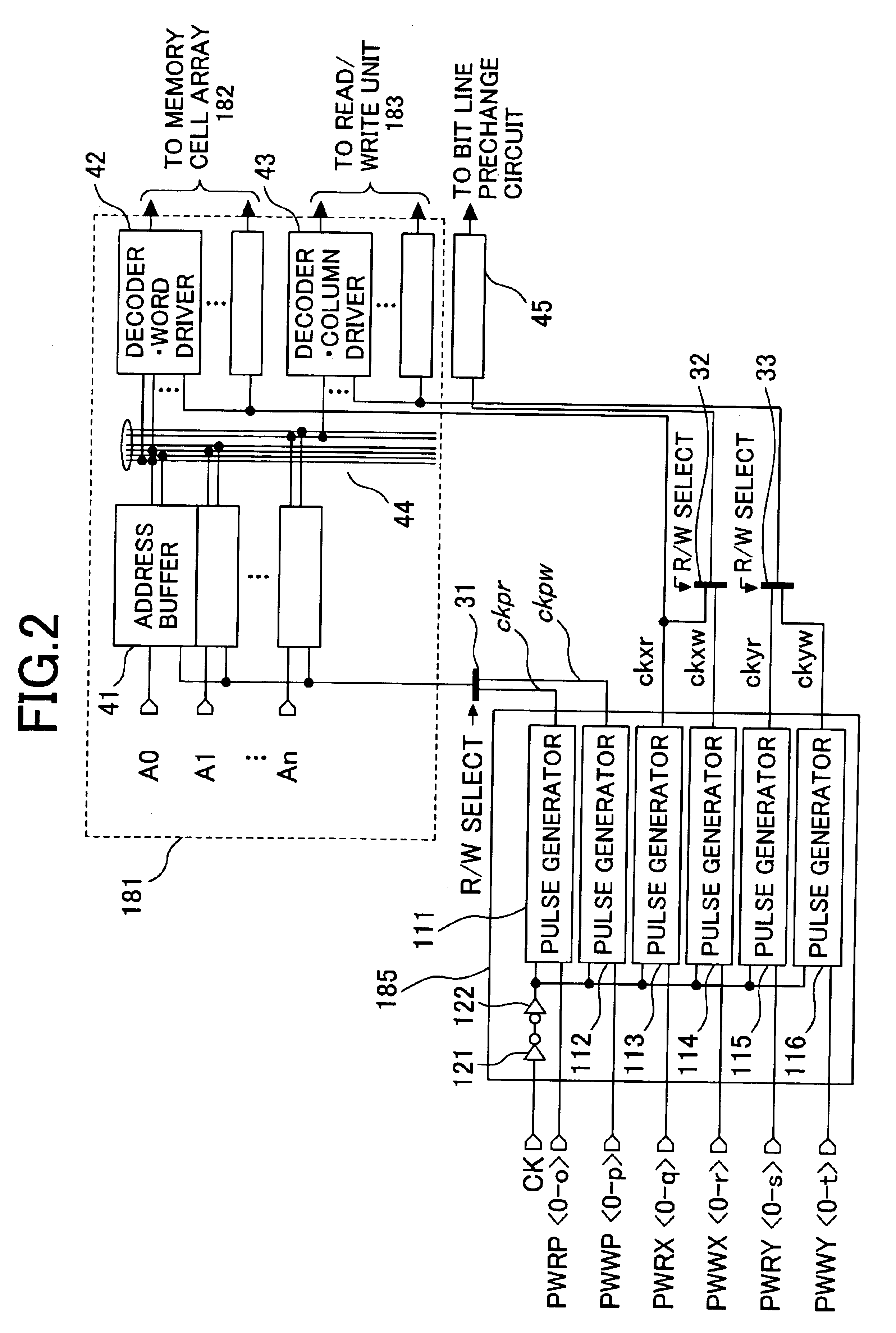
[0043]FIG. 19 is a block diagram showing a still further typical circuit configuration comprising the main components employed in the SRAM;

[0044]FIG. 20 is a diagram showing a typical circuit configuration of a pulse generator employed in the SRAM;

[0045]FIG. 21 is an operation timing diagram of the main components employed in the pulse generator shown in FIG. 20;

[0046]FIG. 22 is a block diagram showing a detailed typical configuration of a clock generator shown in FIGS. 18 and 1; and

[0047]FIG. 23 is a block diagram showing a detailed typical configuration of a clock generator shown in FIG. 5.

DESCRIPTION OF THE PREFERRED EMBODI...


PUM


Abstract

A semiconductor memory device comprises a memory-cell array for storing data, a peripheral circuit for carrying out an operation to read out or write data from or into the memory-cell array, read clock generation circuits (111, 113 and 115) each used for generating a read clock signal to be supplied to the peripheral circuit in the operation to read out data from the memory-cell array, write clock generation circuits (112, 114 and 116) each used for generating a write clock signal to be supplied to the peripheral circuit in the operation to write data into the memory-cell array. Since the pulse widths of the clock signals in read and writes are adjusted individually, margin insufficiencies of the pulse widths can be evaluated and results of the evaluation can be fed back to a design phase for, among other purposes, correction of a layout.

Description

BACKGROUND OF THE INVENTION[0002]1. Field of the Invention[0003]In general, the present invention relates to a semiconductor memory device and a technology capable of evaluating a margin insufficiency of the pulse width of a clock signal in the semiconductor memory device and feeding a result of the evaluation back to a design phase with ease for, among other purposes, correction of the layout of the device based on the result. More particularly, the present invention relates to an effective technology applied to semiconductor memory devices including an SRAM (Static Random Access Memory).[0004]2. Description of the Related Art[0005]Documents such as Japanese Patent Laid-open No. 11-306758 have disclosed a semiconductor memory device comprising: a plurality of bit-line pairs provided for columns of a memory-cell array; a data-line pair for transferring data read out from the memory-cell array; a control means for selecting one of the bit-line pairs and for controlling an operation t...

Claims


Application Information

Patent Timeline
IPC IPC(8): G11C7/00G11C7/22G11C11/413G11C11/417G11C11/41
CPCG11C7/22G11C11/413G11C7/222
Inventor IWAHASHI, SATOSHIHIGETA, KEIICHI
Owner HITACHI LTD
Why Eureka
Try Eureka