Method for designing logic circuit and CAD program

a logic circuit and logic synthesis technology, applied in the field of logic circuit design, can solve the problems of delay logic circuit design, logic synthesis process design period that requires the longest logic synthesis process design period, and increase the logic synthesis process period for achieving desired performance, etc., to achieve the effect of short period of time and low cos

Inactive Publication Date: 2006-09-19
HITACHI LTD
View PDF4 Cites 26 Cited by
  • Summary
  • Abstract
  • Description
  • Claims
  • Application Information

AI Technical Summary

Benefits of technology

[0013]In view of the foregoing problems, it is therefore an object of the present invention to provide a method for designing a logic circuit and a CAD program which ensure security protection without making advanced security provisions. Another object of the present invention is to provide a method for designing a logic circuit and a CAD program which are also compatible with promptly or repeatedl

Problems solved by technology

This causes the problem that, even if a design period is reduced by distributing design resources and increasing the degree of abstractness of a logic description level, the design period of the logic synthesis process for achieving desired performance is increased and the total design period of a whole semiconductor chip cannot sufficiently be reduced.
Accordingly, the delay design of a logic circuit requires a longest design period in the logic synthesis process.
Since the process performed by CAD for logic synthesis is used to solve a so-called combinational optimization problem by searching for an optimal solution closer to a design objective among numerous candidate solutions, it is impossible to select the best one by evaluating all solutions in a practical time.
This frequently causes the situation in which a CAD tool A generates a better circuit with design data A, while a CAD tool B allows the generation of a circuit higher in performance with design data B. Therefore, it is costly and unpractical for one design site to purchase a variety of CAD tools for synthesis.
If this form of business service is us

Method used


Image

  • Method for designing logic circuit and CAD program
  • Method for designing logic circuit and CAD program
  • Method for designing logic circuit and CAD program

Examples


Embodiment Construction

[0026]Referring to the drawings, an embodiment of the present invention will be described herein below.

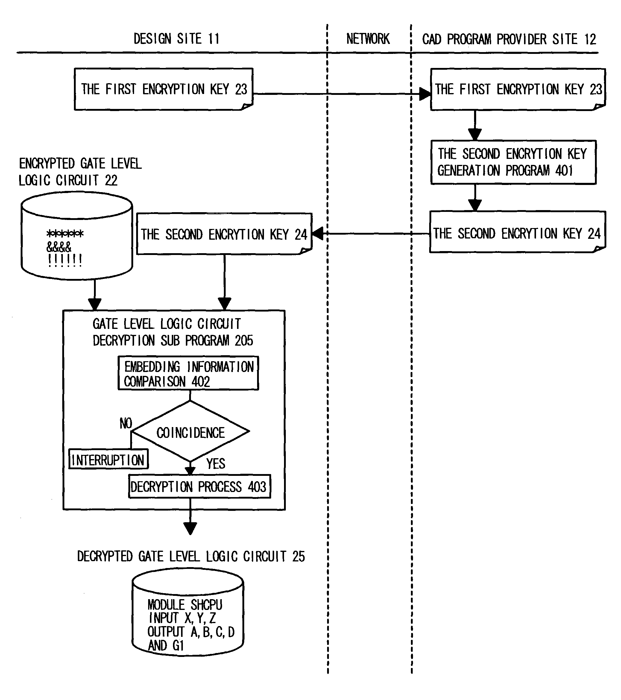
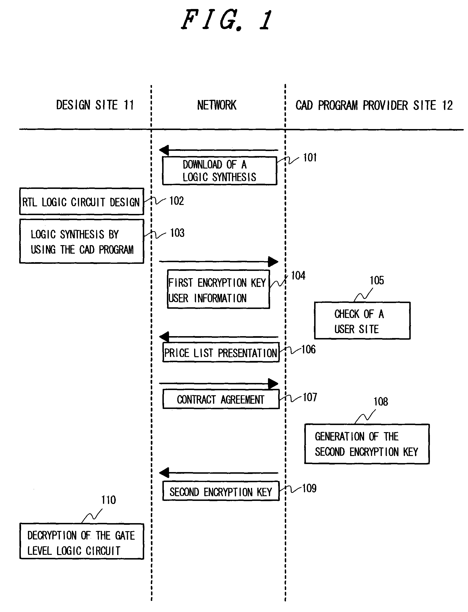
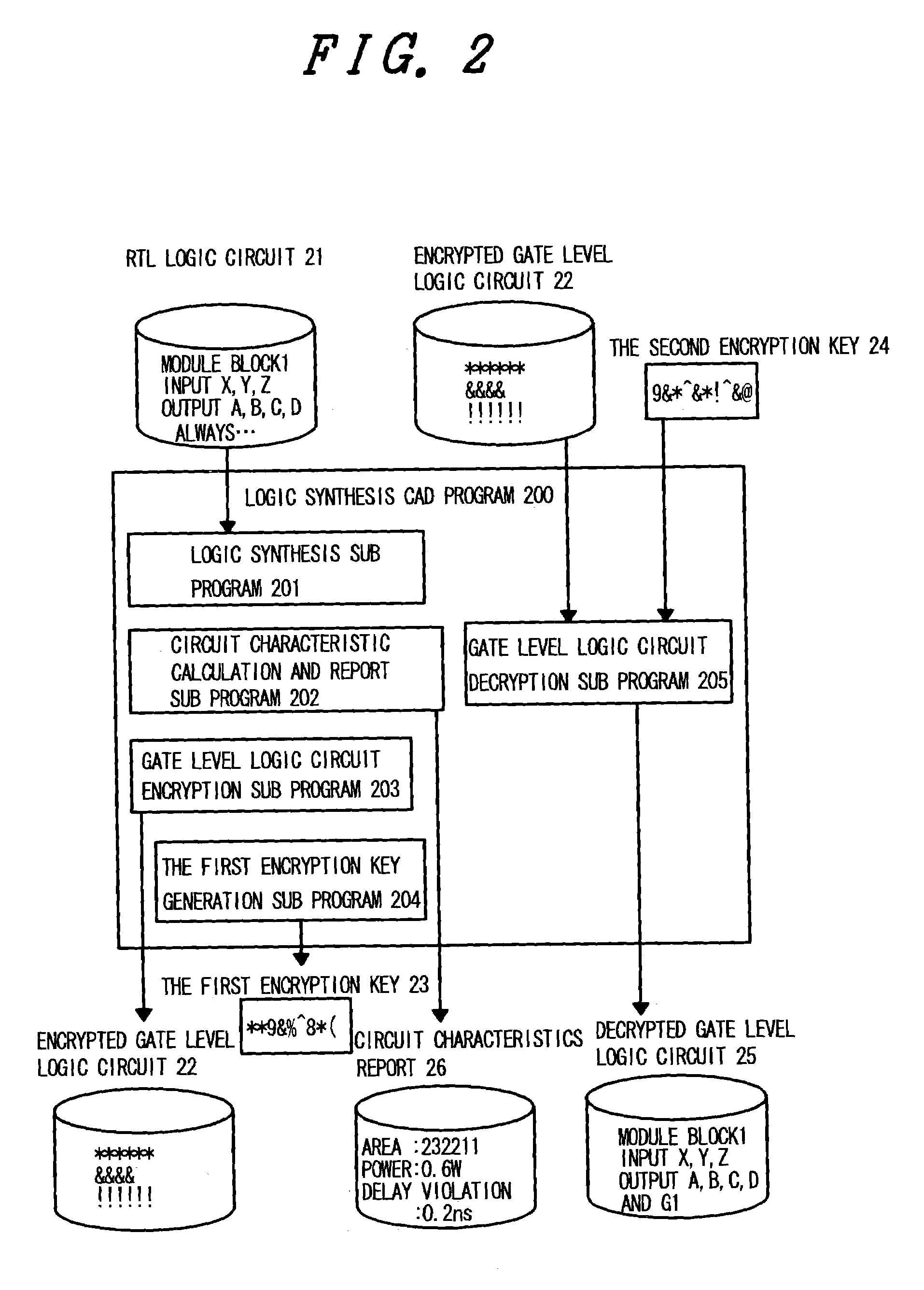
[0027]FIG. 1 shows the embodiment of a design method according to the present invention. In an example shown in the drawing, a network provides connection between a design site 11 and a CAD program provider site 12 so that design is performed through the network. In the drawing, the box underlying the design site, the box underlying the CAD program provider site, and the box underlying the network represent a process performed at the design site, a process performed at the CAD program provider site, and information transmitted by communication performed via the network, respectively. First, the design site acquires a CAD program at no charge by downloading it from the CAD program provider site (101). It will be understood that this communication is unnecessary if the design site has already acquired the CAD program. The CAD program may also be acquired by means other than downloadi...


PUM


Abstract

A method for designing a logic circuit and a CAD program which allow a logic circuit with desired performance to be designed in a short period of time by suppressing the elongation of a logic design period for achieving a circuit area, an operating speed, power consumption, and the like as target specifications are provided at low cost. Shorter-period and lower-cost design is accomplished by allowing a user to use a high-performance logic synthesis CAD program at no charge if he only checks circuit characteristics resulting from synthesis and collecting a fee if the user is satisfied with the resulting circuit characteristics and intends to use a gate level logic circuit. In a design phase which receives a register transfer level or operation level logic circuit and synthesizes a gate level logic circuit, desired circuit characteristics are obtainable in a short period of time at low cost.

Description

BACKGROUND OF THE INVENTION[0001]1. Field of the Invention[0002]The present invention relates to a method for designing a logic circuit and, more particularly, to a method for designing a high-performance logic circuit in a short period of time.[0003]2. Description of Related Art[0004]In the current design of a logic circuit, a method in which a logic function is described at a register transfer level or an operation level in a logic description language termed an HDL (Hardware Description Language) and the logic described at the register transfer level or the operation level is converted to gate level logic by using a CAD tool for logic synthesis is used most prevalently. The register transfer level explicitly describes required registers and arithmetic units in conjunction with data paths and control paths for providing connection between the registers and the arithmetic units. At present, the register transfer level is a description level used most frequently for a logic circuit ...

Claims


Application Information

Patent Timeline
IPC IPC(8): G06F17/50G09C1/00H04L9/08
CPCG06F17/5045G06F2217/78G06F30/30G06F2119/06
Inventor KATO, NAOKIYANO, KAZUO
Owner HITACHI LTD
Why Eureka
Try Eureka