

Semiconductor apparatus
a technology of semiconductors and circuits, applied in semiconductor/solid-state device testing/measurement, pulse techniques, instruments, etc., can solve problems such as failure of internal circuits that receive potentials based on primary reference potentials to function correctly, failure to latch up, and failure to destroy devices under tes
- Summary
- Abstract
- Description
- Claims
- Application Information
AI Technical Summary
Benefits of technology
Problems solved by technology
Method used
Image

Examples
Embodiment Construction
Various embodiments of the present invention will now be described in detail with reference to a number of drawings.
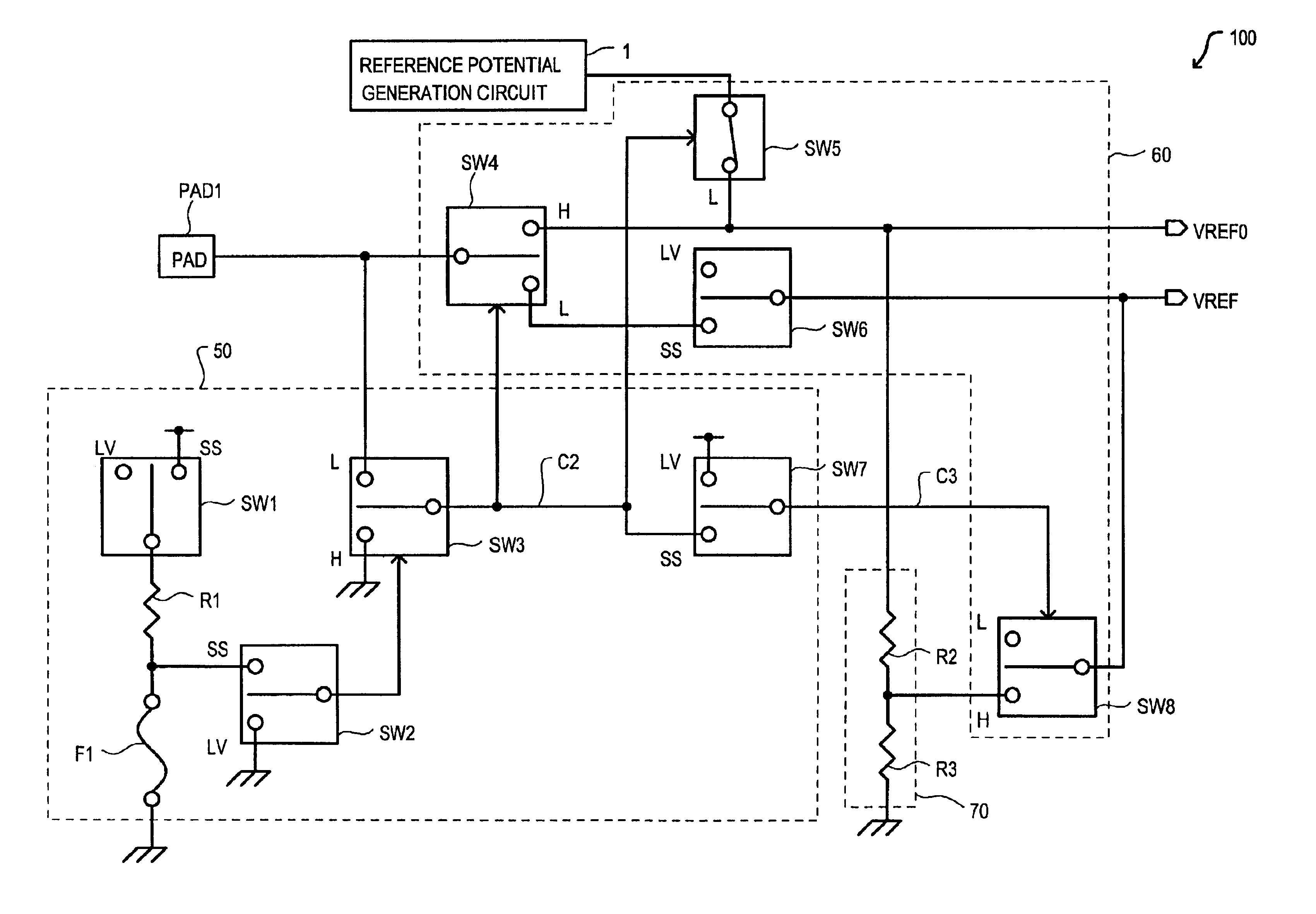
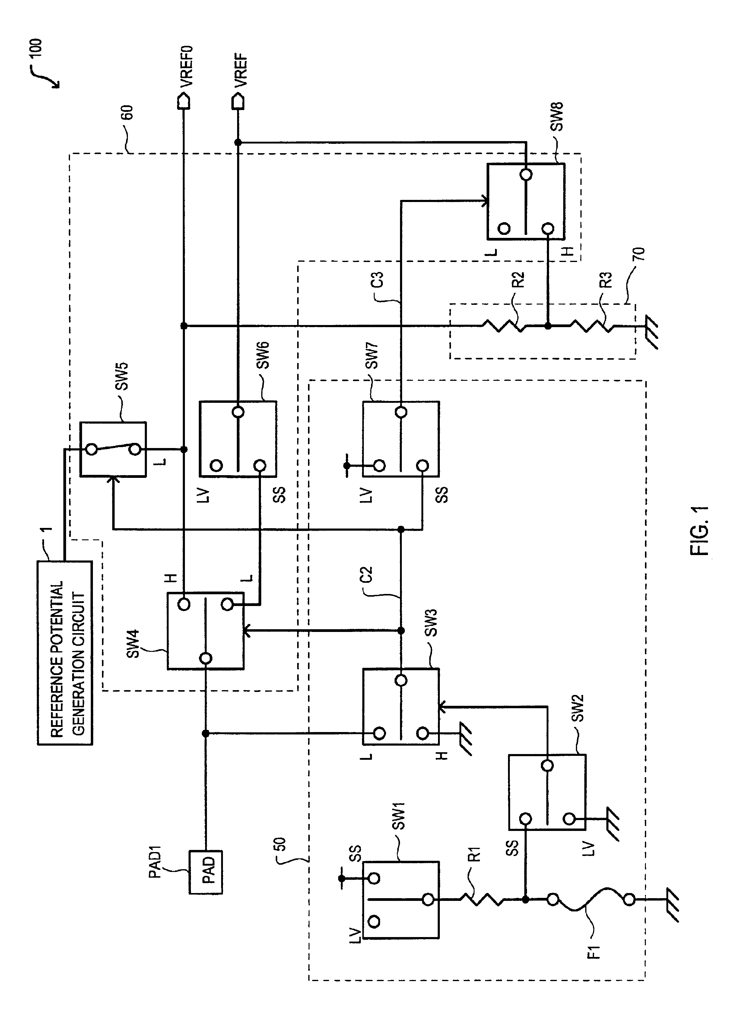
Referring now to FIG. 1, a circuit schematic diagram of a reference configuration circuit according to an embodiment is set forth and given the general reference character 100.
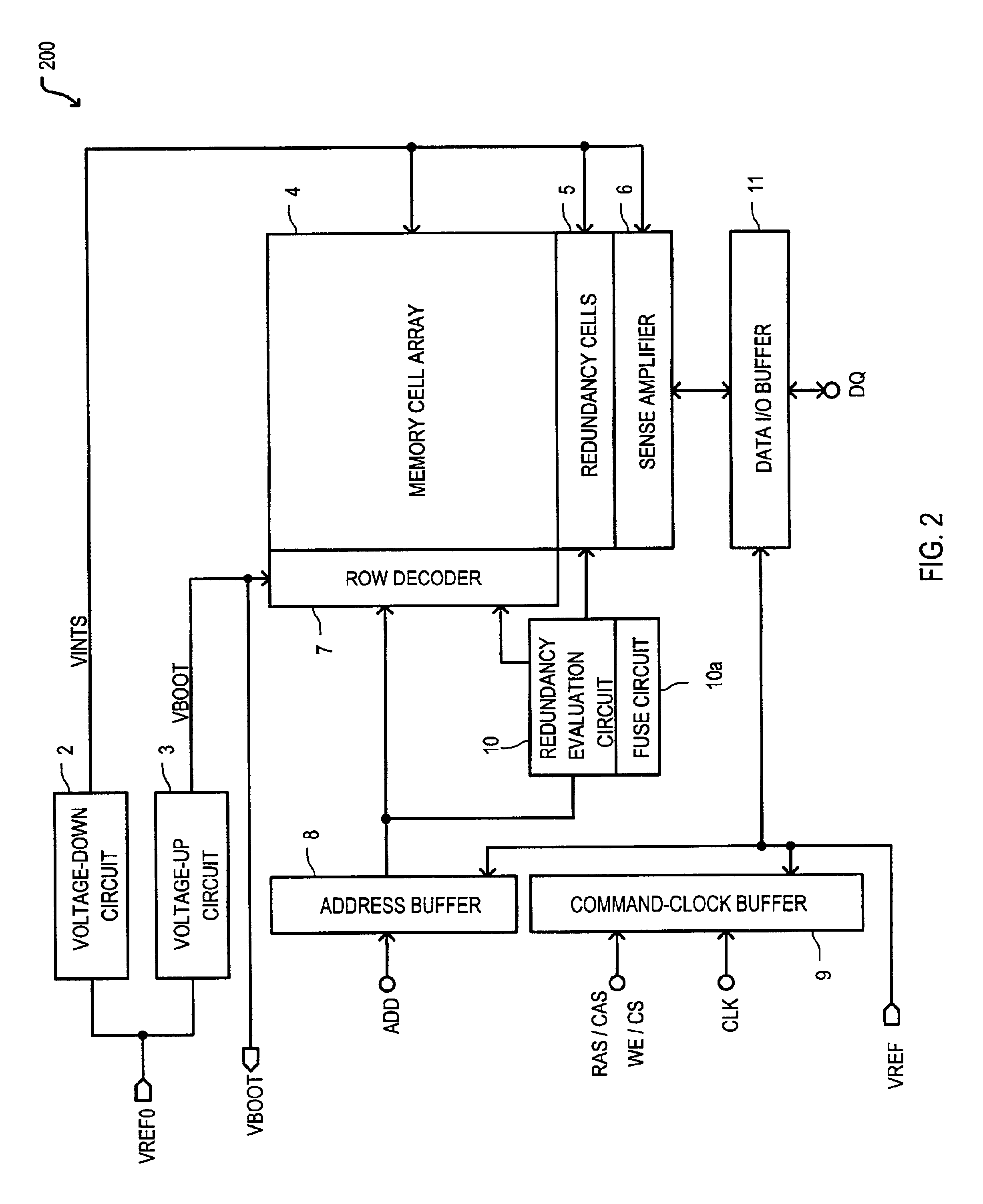
Reference configuration circuit 100 can include, a bond pad PAD1, a reference potential generation circuit 1, a control circuit 50, a reference selection circuit 60, and a secondary reference potential generation circuit 70. Reference configuration circuit 100 may receive an input signal from bond pad PAD1 and may provide a primary reference potential VREF0 and a secondary reference potential VREF.
Reference configuration circuit 100 may provide a primary reference potential VREF0 and a secondary reference potential VREF determined by a mode of operation of a semiconductor device and a potential that may be applied to bond pad PAD1. A semiconductor device incorporating reference configuration circ...
PUM
 Abstract
Description
Claims
Application Information