Non-switched capacitor offset voltage compensation in operational amplifiers

an offset voltage compensation and non-switched capacitor technology, applied in differential amplifiers, amplifiers with semiconductor devices/discharge tubes, amplifier details, etc., can solve the problems of not attractive approaches, pure digital cmos processes do not characterize these values, and the offset voltage compensation is not suitable for operation. , to achieve the effect of minimizing delay and minimizing inaccuracy

Inactive Publication Date: 2005-02-22
STMICROELECTRONICS PVT LTD
View PDF6 Cites 6 Cited by
  • Summary
  • Abstract
  • Description
  • Claims
  • Application Information

AI Technical Summary

Benefits of technology

The means / unit for disconnecting phase compensation circuitry, if any, and operating the operational amplifier as a comparator during the calibration mode are provided, so as to minimize delay. The mechanism for automatically determining tap selection in the resistor chain is any known successive approximation technique. The tapped resistor chain is made using a single resistor strip with side taps, so as to minimize inaccuracies due to finite contact resistances.

Problems solved by technology

Typically, opamps exhibit certain limitations, the most important of which is the offset voltage.
There is a technique used in discrete opamp ICs, where an external potentiometer is used to nullify the offset voltage; but this technique needs two more pins, which is not an attractive approach when an opamp is just a part of a big chip with limited pin-outs.
Unfortunately, pure digital CMOS processes do not characterize these values.
A separate DAC, extra comparator and opamp (for V2I) are needed, and it suffers from consumption and area overhead.
This method also suffers from constant consumption in the current divider, which does not contribute to the opamp.

Method used


Image

  • Non-switched capacitor offset voltage compensation in operational amplifiers
  • Non-switched capacitor offset voltage compensation in operational amplifiers
  • Non-switched capacitor offset voltage compensation in operational amplifiers

Examples


Embodiment Construction

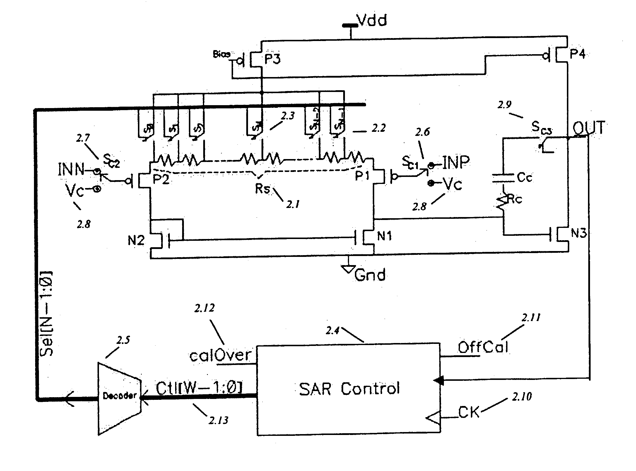
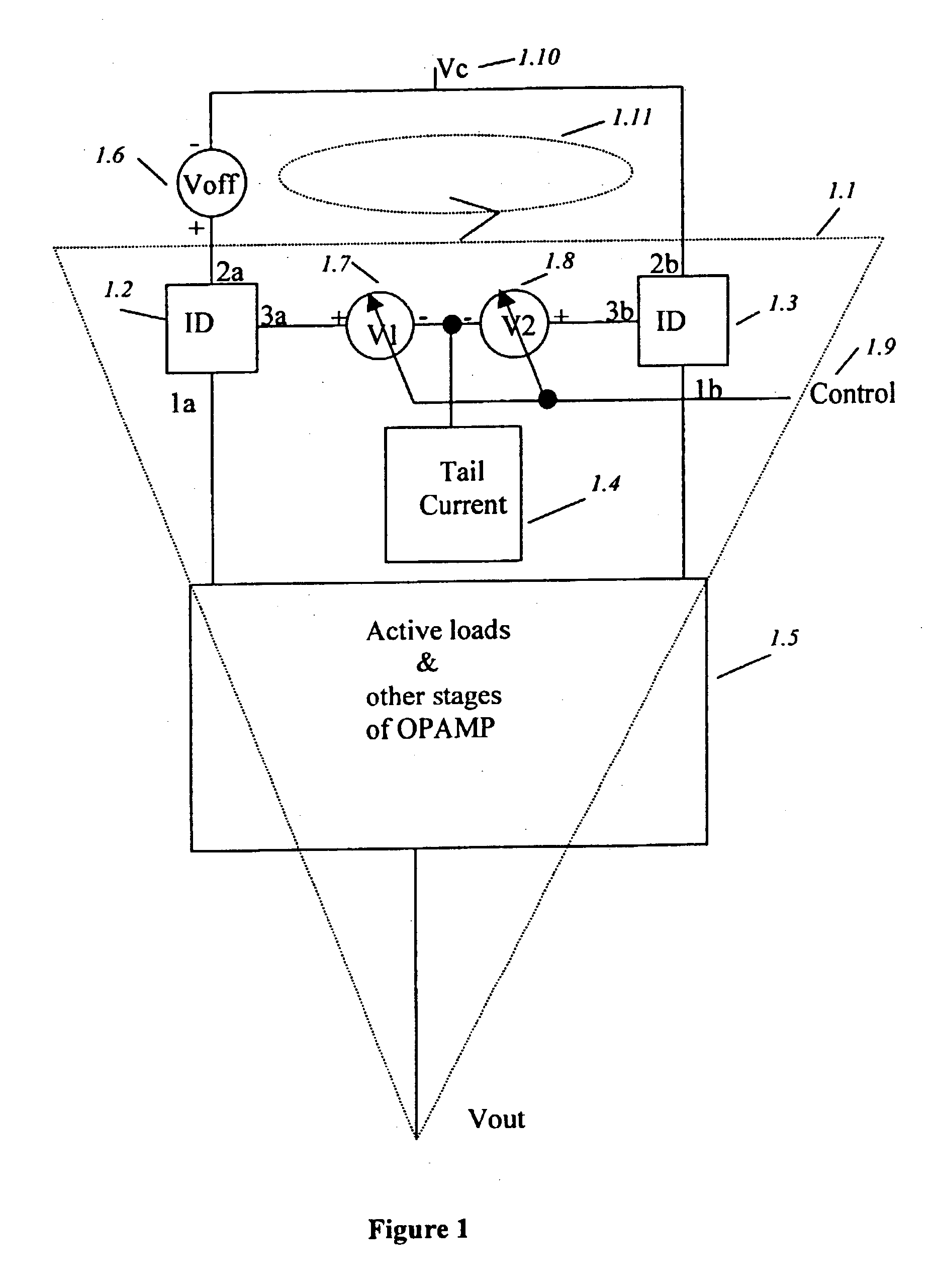
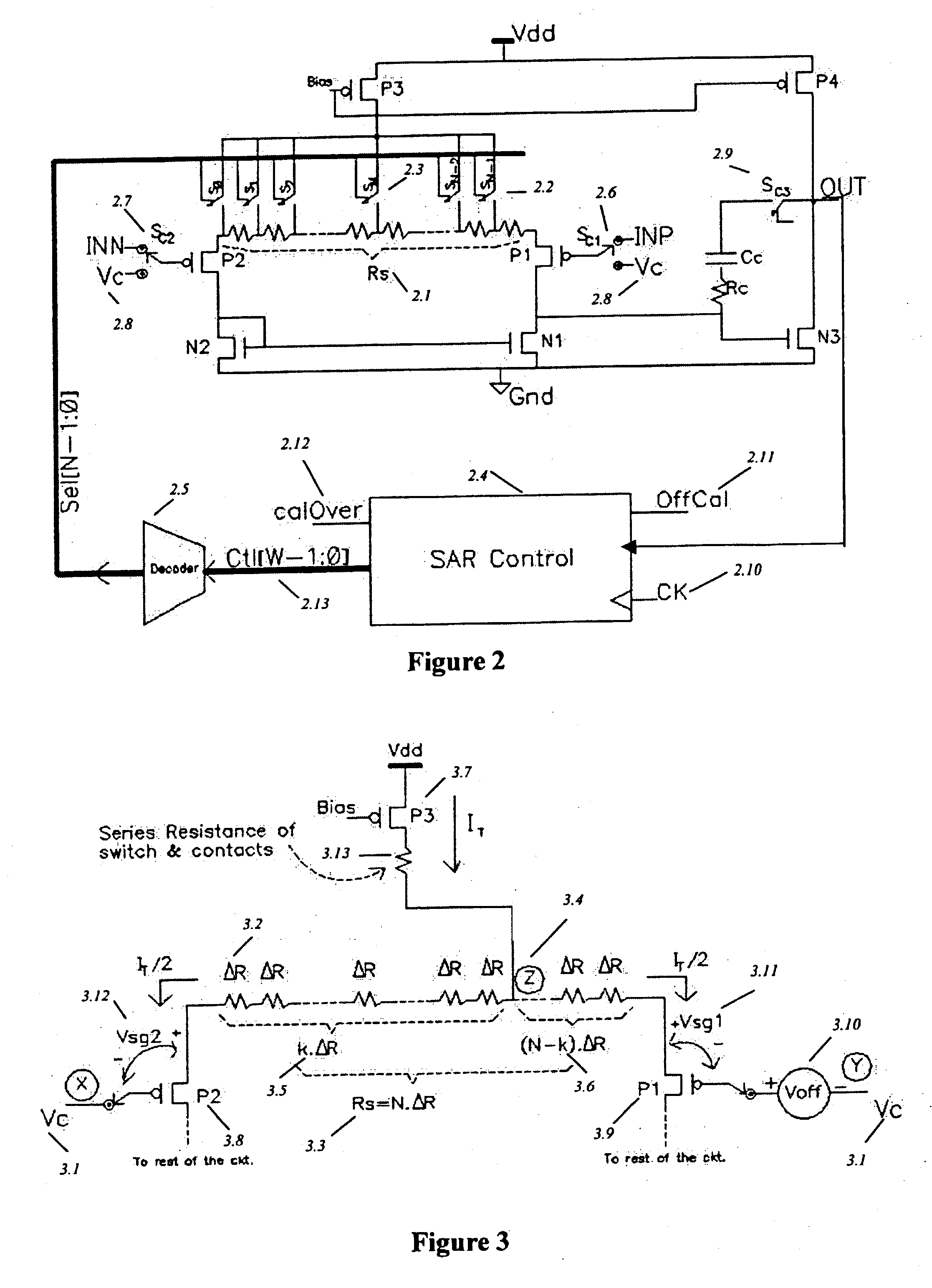
FIG. 1 shows the block diagram of an opamp. Different components of an OPAMP (inside the dashed lines [1.1]) are shown as blocks. The IDs [1.2, 1.3] are the input devices of the differential stage of the OPAMP, which can be N or P type MOS or NPN or PNP bipolar devices. Tail current [1.4], active loads and following stages [1.5] are shown as different boxes. The offset voltage caused by different mismatches and non-idealities, is referred to the input (outside OPAMP) as Voff [1.6], so that the components of the OPAMP are considered to be matched. The offset voltage due to the differential amplifier only is determined by: Voff=Δ⁢ ⁢Vtdiff+Δ⁢ ⁢Vtload⁡(gmloadgmdiff)+Δ⁡(Vgs-Vt)⁢diff2·[-Δ⁢ ⁢(W / L)diff(W / L)diff-Δ⁢ ⁢(W / L)load(W / L)load](1)

To nullify the effect of Voff to an ideal OPAMP, two controllable voltage drops, V1 [1.7]& V2 [1.8], are introduced between terminal 3a and tail current and between 3b and tail current respectively (where 3a &3b are sources in the case of a MOS input device ...


PUM


Abstract

A method for reducing offset voltage in an operational amplifier without the need for switched-capacitors, includes introducing a tapped resistor chain between the common connected terminals of the transistors of the input differential pair of the operational amplifier and connecting the tail current source/sink of the differential amplifier to a selected tap of the resistor chain. The invention further provides an improved operational amplifier in accordance with the above method.

Description

FIELD OF THE INVENTIONThe present invention relates to non-switched capacitor offset voltage compensation in operational amplifiers, and is suitable for digital processes where the analog characteristics of the process are not defined.BACKGROUND OF THE INVENTIONOperational amplifiers (opamps) are very widely used analog components. Their versatility makes them a building block for several applications. Typically, opamps exhibit certain limitations, the most important of which is the offset voltage. The offset voltage of an opamp is the differential voltage required to be applied at the input of the opamp to produce a null output. Many applications require the cancellation / minimization of the offset voltage.There are a few well-known approaches to reduce / cancel the input referred offset or the effect of input referred offset in the opamps. If the opamp is used in the switched capacitor circuit, then offset voltage is stored in the capacitors connected to the input of the opamp during...

Claims


Application Information

Patent Timeline
Patent Type & Authority Patents(United States)
IPC IPC(8): H03F3/45
CPCH03F3/45753
Inventor NANDY, TAPASRATHORE, KIRTIMAN SINGH
Owner STMICROELECTRONICS PVT LTD
Why Eureka
Try Eureka