
Electrophoretic display

a display and electrophoretic technology, applied in the field of electrophoretic display, can solve the problems of reducing the life or stability of the electrophoretic display as a display apparatus, affecting the display stability, and affecting the display stability, and achieve the effect of excellent display stability and high-contrast display

Inactive Publication Date: 2005-03-01
CANON KK
View PDF13 Cites 28 Cited by
  • Summary
  • Abstract
  • Description
  • Claims
  • Application Information

AI Technical Summary

Benefits of technology

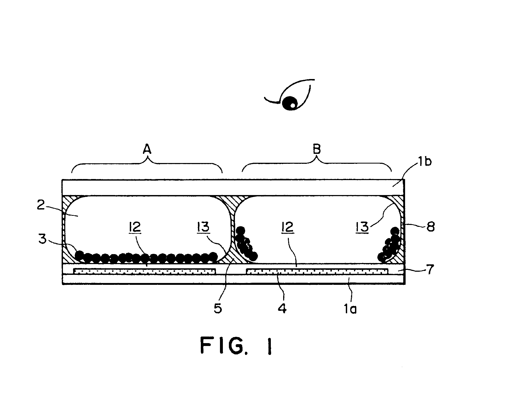
An object of the present invention is to provide an electrophoretic display which is excellent in display stability and is capable of realizing high-contrast display.

Problems solved by technology

However, such a electrophoretic display is accompanied with a problem such that a display irregularity liable to occur due to mutual agglomeration or localization of the colored and charged electrophoretic particles 3.
As a result, donation and acceptation of electric charges due to the color former used as caused to occur, thus adversely affecting an electrophoretic operation of the charged electrophoretic particles to cause a problem such that the life or stability of the electrophoretic display as a display apparatus is lowered.
As a result, a high contrast state is not readily realized.
More specifically, an electric field created within one microcapsule is leaked to an adjacent microcapsule, thus adversely affecting movement of the charged electrophoretic particles within the microcapsules.

Method used


Image

  • Electrophoretic display
  • Electrophoretic display
  • Electrophoretic display

Examples


example 1

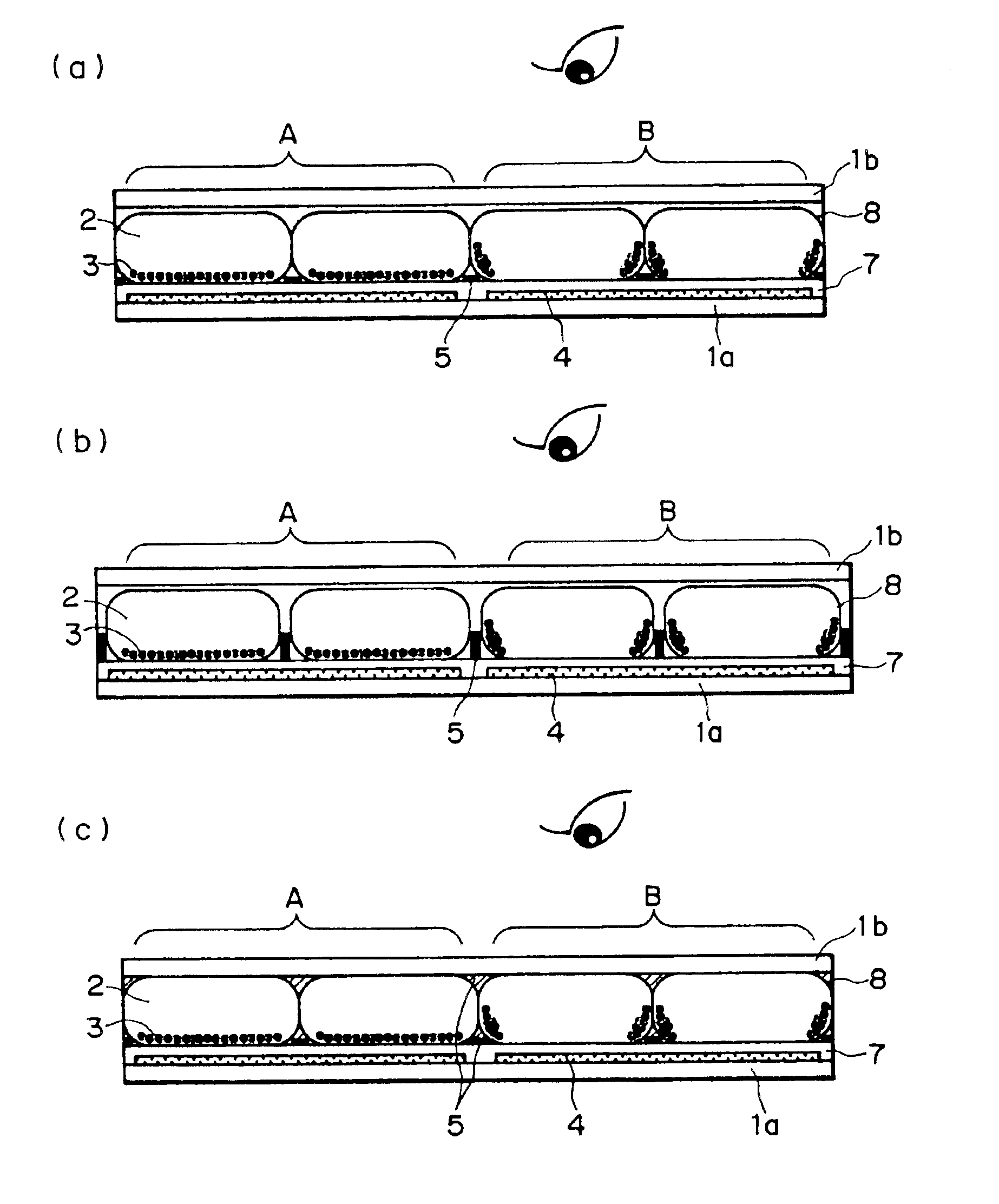
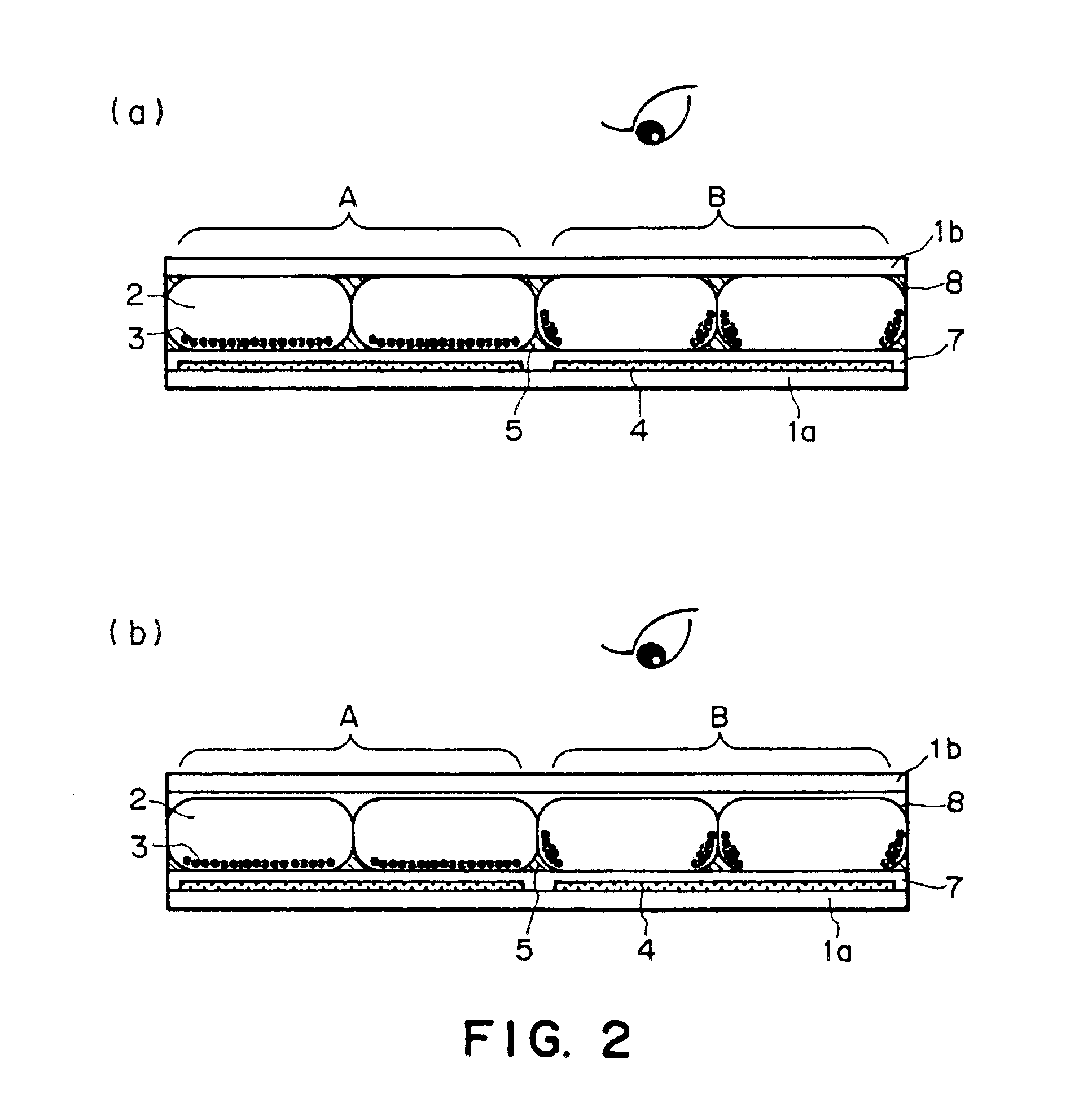
An electrophoretic display having a structure shown in FIG. 1 was prepared by the above-mentioned first production process shown in FIG. 7.

The size of each (one) pixel was set to 100 μm×100 μm.

As a first substrate 1a, an aluminum thin film was formed on a surface of a (200 μm-thick) PET film, followed by patterning through a photo-lithographic or wet etching process to form a plurality of first electrodes 4. White coloring layers were formed so as to cover these first electrodes 4. These white coloring layers 4 were formed of an acrylic resin and a white pigment, such as titanium oxide (used in this example) or alumina, dispersed in the acrylic resin.

Then, an insulating layer 7 of an acrylic resin was formed so as to cover the white coloring layers.

Microcapsules 8 were prepared by a combined coacervation method. As an insulating liquid 2, isoparaffin (trade name: “Isopar”, mfd. by Exxon Corp.) was used, and as charged electrophoretic particles 3, particles of polystyrene-polymethyl ...

example 2

An electrophoretic display having a structure shown in FIG. 3(b) was prepared in the following manner.

The size of each (one) pixel was set to 180 μm×180 μm.

As a first substrate 1a, an aluminum thin film was formed on a surface of a (180 μm-thick) PES film, followed by patterning through a photo-lithographic or wet etching process to form a plurality of first electrodes 4. White coloring layers were formed so as to cover these first electrodes 4. These white coloring layers 4 were formed of an acrylic resin and a white pigment, such as titanium oxide (used in this example) or alumina, dispersed in the acrylic resin.

Then, an insulating layer 7 of an acrylic. resin was formed so as to cover the white coloring layers.

Onto the entire surface of the insulating layer 7, an electroconductive resist was applied, followed by patterning in a shape shown in FIG. 3(b) to form a second electrode having a width of 5 μm and a height of 15 μm. As the electroconductive resist, it is possible to use t...

example 3

An electrophoretic display having a structure shown in FIG. 3(c) was prepared by the fifth production process shown in FIG. 9.

The size of each (one) pixel was set to 180 μm×180 μm.

As a first substrate 1a, an aluminum thin film was formed on a surface of a (1.1 mm-thick) glass substrate, followed by patterning through a photo-lithographic or wet etching process to form a plurality of first electrodes 4. White coloring layers were formed so as to cover these first electrodes 4. These white coloring layers 4 were formed of an acrylic resin and a white pigment, such as titanium oxide (used in this example) or alumina, dispersed in the acrylic resin.

Then, an insulating layer 7 of an acrylic resin was formed so as to cover the white coloring layers.

Then, on the surface of the insulating layer 7, an ITO (indium tin oxide) film was formed, followed by patterning through a photolithographic or wet etching process to form a plating electrode 51 having a width of 5 μm.

Microcapsules 8 were prep...


PUM

PropertyMeasurementUnit
heightaaaaaaaaaa
heightaaaaaaaaaa
particle sizeaaaaaaaaaa

Abstract

An electrophotographic display includes a plurality of microcapsules each encapsulating therein an insulating liquid and a plurality of charged electrophoretic particles dispersed in the insulating liquid, a first substrate and a second substrate disposed opposite to each other so as to sandwich the plurality of microcapsules, and a plurality of electrodes capable of being supplied with a voltage. A voltage is applied between the plurality of electrodes to move the charged electrophoretic particles between a first internal wall portion of each microcapsule an external surface of which contacts the first substrate and a second internal wall portion of each microcapsule an external surface of which is substantially out of contact with both the first and second substrate, thereby to switch a display state.

Description

FIELD OF THE INVENTION AND RELATED ARTThe present invention relates to an electrophoretic display (apparatus) for performing display by moving charged electrophoretic particles (charged migrating particles) and a process for producing the electrophoretic display.With remarkable progress of digital technologies an amount of personally available information has been rapidly increased, so that low-power-consumption and thin-shaped display apparatuses have been developed actively as information output means.One of such display apparatus has been proposed as an electrophoretic display by U.S. Pat. No. 3,612,758.FIG. 11 shows an embodiment of a structure of the electrophoretic display D2. Referring to FIG. 11, the electrophoretic display D2 of the type includes a pair of substrates 1a and 1b oppositely disposed with a predetermined spacing, an insulating liquid 2 filled between these substrates 1a and 1b, a multitude of colored and charged electrophoretic particles 3 dispersed in the insu...

Claims


Application Information

Patent Timeline
Patent Type & Authority Patents(United States)
IPC IPC(8): G02F1/01G02F1/167G02F1/16757
CPCG02F1/167G02F1/16757
Inventor MATSUDA, YOJIROMATSUDA, HIROSHI
Owner CANON KK
Learn More