Non-volatile memory cell with gated diode and MOS transistor and method for using such cell

a technology of gated diodes and transistors, applied in the field of non-volatile memory cells, can solve the problem that the array of such cells cannot be implemented with sufficient density for many applications

Active Publication Date: 2005-03-01
NAT SEMICON CORP
View PDF5 Cites 33 Cited by
  • Summary
  • Abstract
  • Description
  • Claims
  • Application Information

AI Technical Summary

Problems solved by technology

US 2004/0080982, which requires that one transistor is implemented in N-type semiconductor material (e.g., in an N-well) and the other in P-type semiconductor material

Method used


Image

  • Non-volatile memory cell with gated diode and MOS transistor and method for using such cell
  • Non-volatile memory cell with gated diode and MOS transistor and method for using such cell
  • Non-volatile memory cell with gated diode and MOS transistor and method for using such cell

Examples


Embodiment Construction

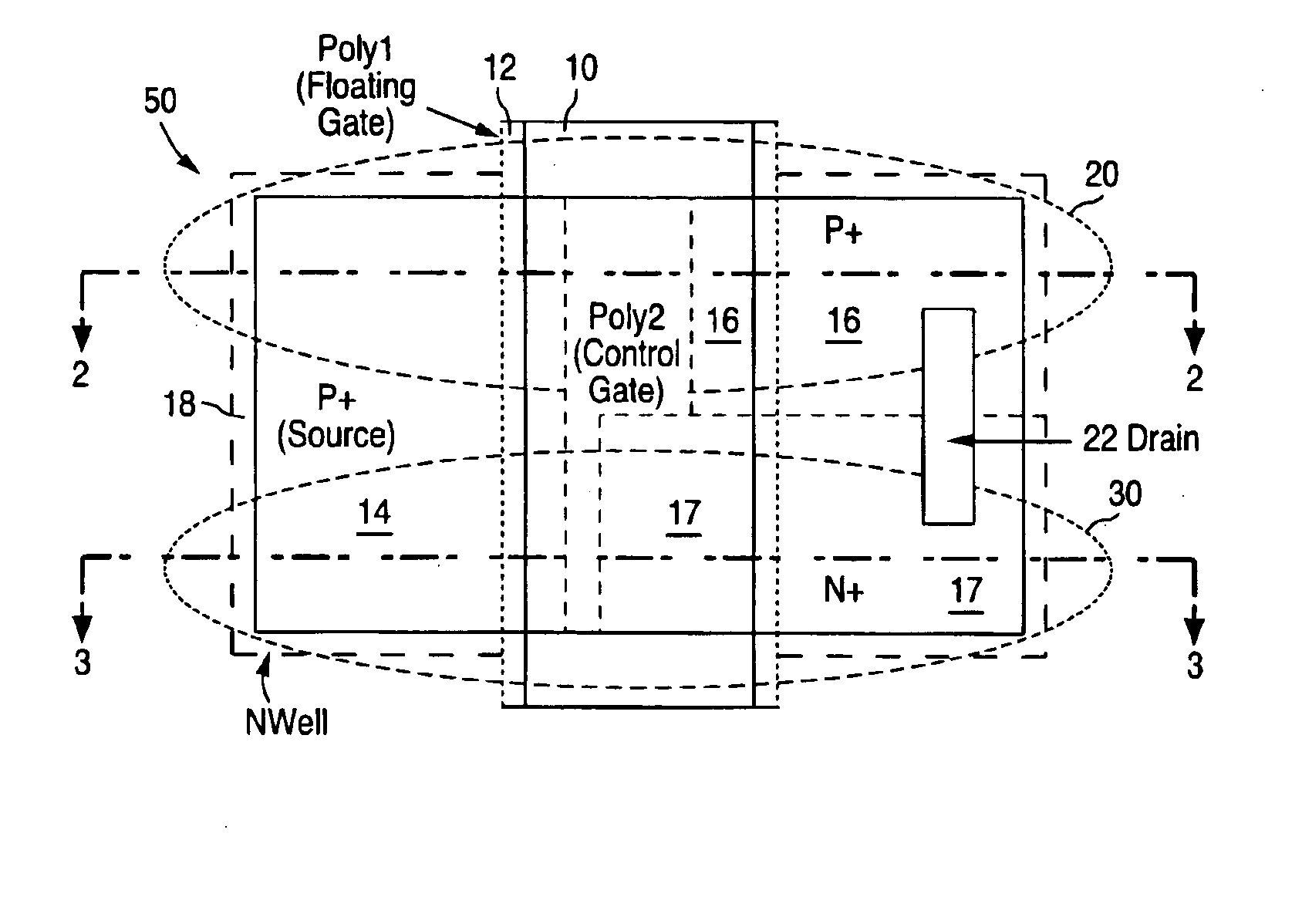
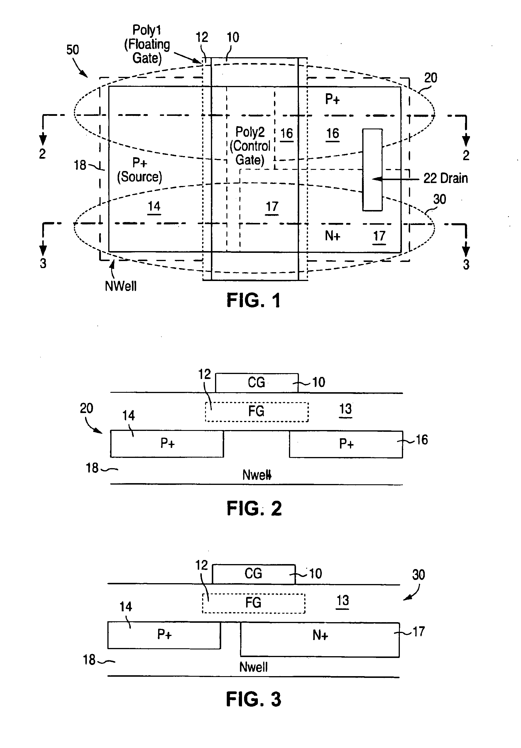
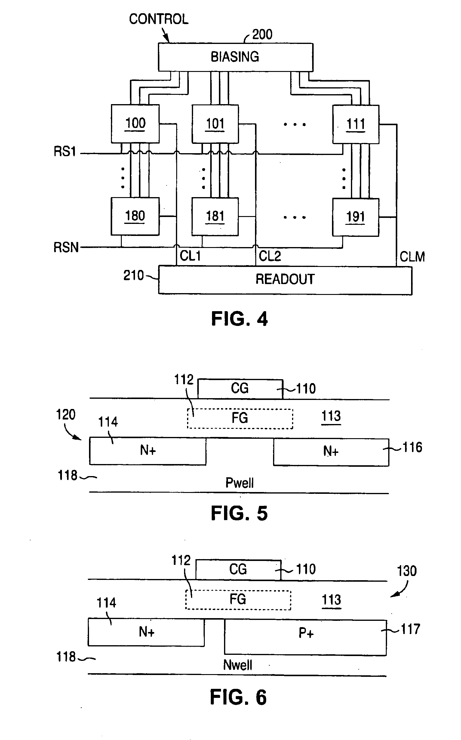
[0011]In a class of embodiments, the invention is a non-volatile memory cell that includes a single readout transistor and a gated diode. The readout transistor is an MOS transistor, and both the MOS transistor and the gated diode are formed in a volume of semiconductor material of one type. For example, the MOS transistor and gated diode are both formed in a well of N-type semiconductor material, or in a well of P-type semiconductor material. The MOS transistor and gated diode share a source region (comprising semiconductor material of one type), a control gate, and a floating gate. The transistor has a drain region (comprising semiconductor material of one type) and the diode has a drain region (comprising semiconductor material of the opposite type). The two drain regions are shorted together (connected by electrically conductive material), and thus the drain regions and conductive material that connects them are sometimes referred to collectively herein as “the” drain of the cel...


PUM


Abstract

A non-volatile memory cell including a gated diode and a single readout transistor, methods for programming and reading out such a cell, and a memory including an array of such cells. The readout transistor is an MOS transistor. The transistor and gated diode are formed in a volume of semiconductor material of one type, and share a source region, a control gate, and a floating gate. The transistor has a drain region formed of semiconductor material of one type and the diode has a drain region formed of semiconductor material of the opposite type.

Description

BACKGROUND OF THE INVENTION[0002]1. Field of the Invention[0003]The present invention pertains to non-volatile memory cells (e.g., non-volatile memory cells that include at least one MOS transistor) and to methods of programming, erasing, and reading them.[0004]2. Description of the Related Art[0005]The expression “PMOS transistor” herein denotes a P-channel MOSFET device. The expression “NMOS transistor” herein denotes an N-channel MOSFET device.[0006]The term “N-well” herein denotes a well of N-type semiconductor material. The term “P-well” herein denotes a well of P-type semiconductor material.[0007]One type of conventional non-volatile memory cell is described in U.S. Pat. No. 4,698,787, issued Oct. 6, 1987. This cell includes a single MOS transistor having a stacked gate structure. The stacked gate structure includes a control gate, a floating gate, a dielectric layer insulating the control gate from the floating gate, and additional dielectric material (gate oxide) insulating ...

Claims


Application Information

Patent Timeline
IPC IPC(8): G11C16/04H01L29/66H01L29/788H01L29/861
CPCG11C16/0416H01L29/8616H01L29/7881
Inventor HOPPER, PETER J.MIRGORODSKI, YURIVASHCHENKO, VLADISLAV
Owner NAT SEMICON CORP
Why Eureka
Try Eureka