Magnetic random access memory having flux closure for the free layer and spin transfer write mechanism

a random access memory and free layer technology, applied in the field of magnetic random access memories, can solve the problems of limiting the cell packing density, unable to reach the commercial market, and the stabilization of a finite moment fl into a single domain state,

Inactive Publication Date: 2005-03-08
SEAGATE TECH LLC
View PDF24 Cites 65 Cited by
  • Summary
  • Abstract
  • Description
  • Claims
  • Application Information

AI Technical Summary

Problems solved by technology

MRAM technology is still in its infancy and has yet to reach the commercial market.
However, the stabilization of a finite moment FL into a single domain state presents a challenge because of the need to combat energetically prohibitive free magnetic charges at the surface of the FL.
Even when a stable single domain state is achieved, the magnetostatic fields generated by the FL will interact with neighboring magnetoresistive elements, thereby limiting the packing density of cells.
Flux closure is therefore a significant issue affecting the reproducibility of single domain bits, but a finite moment FL is an unavoidable obstacle for those MRAM designs that write bits with magnetic fields.
But, these proposals still require a net moment for the FL and are only a stopgap solution to the problem.
However, these proposals provide only a partial solution because the proposed SAF structures require a net moment in order to work properly in the magnetic fields of the intended application.

Method used


Image

  • Magnetic random access memory having flux closure for the free layer and spin transfer write mechanism
  • Magnetic random access memory having flux closure for the free layer and spin transfer write mechanism
  • Magnetic random access memory having flux closure for the free layer and spin transfer write mechanism

Examples


Embodiment Construction

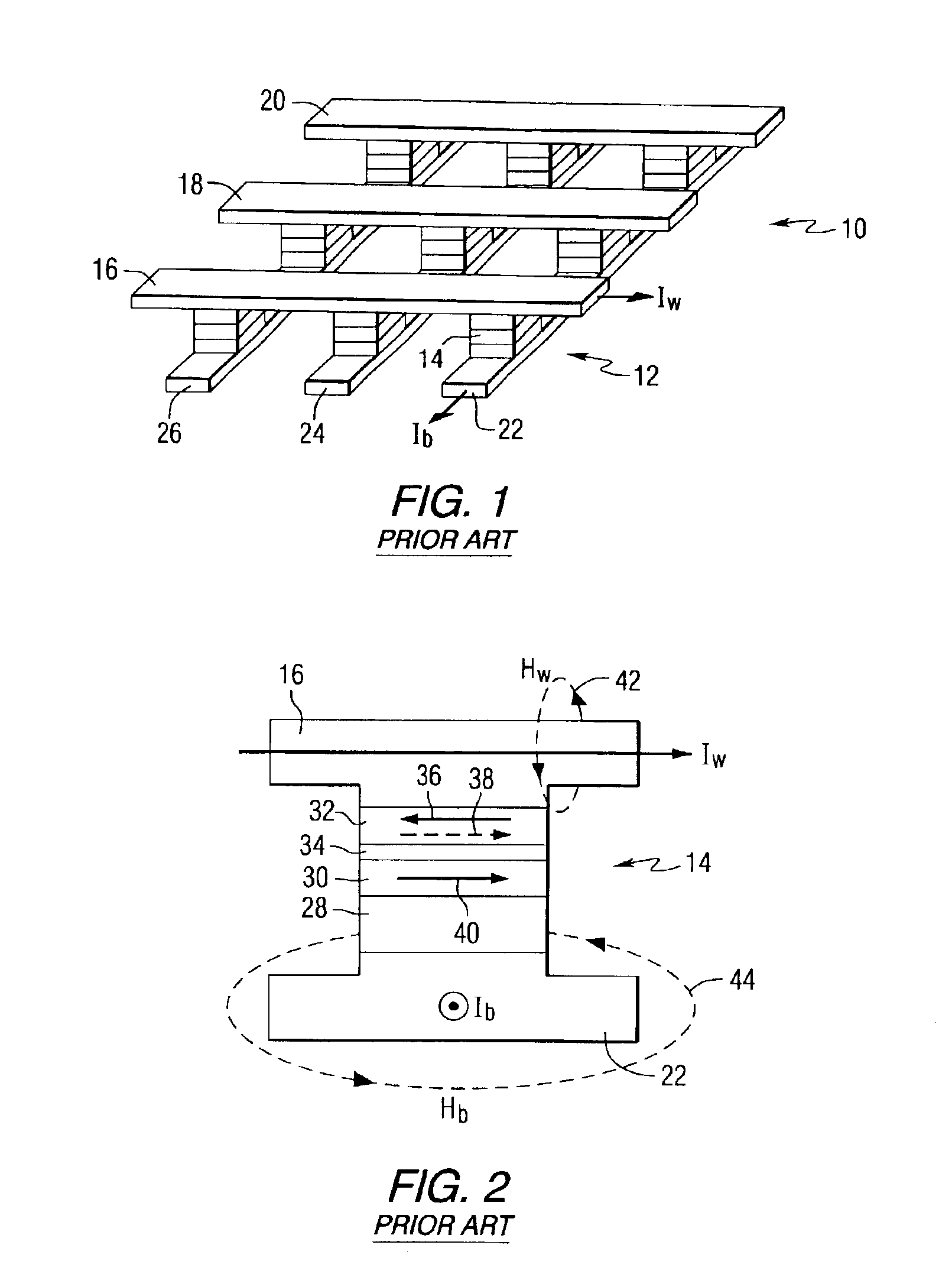
Referring to the drawings, FIG. 1 is a schematic representation of a conventional magnetic random access memory 10. MRAM 10 includes a 3×3 array of cells 12 that are a subset of the total number of cells comprising the MRAM device. Every cell contains one MR element 14. There are two roughly orthogonal sets of electrical wires, referred to as word lines 16, 18 and 20, and bit lines 22, 24 and 26, that overlap the MR elements. A bit is written only at the intersection of the word and bit lines that have current flowing through them.

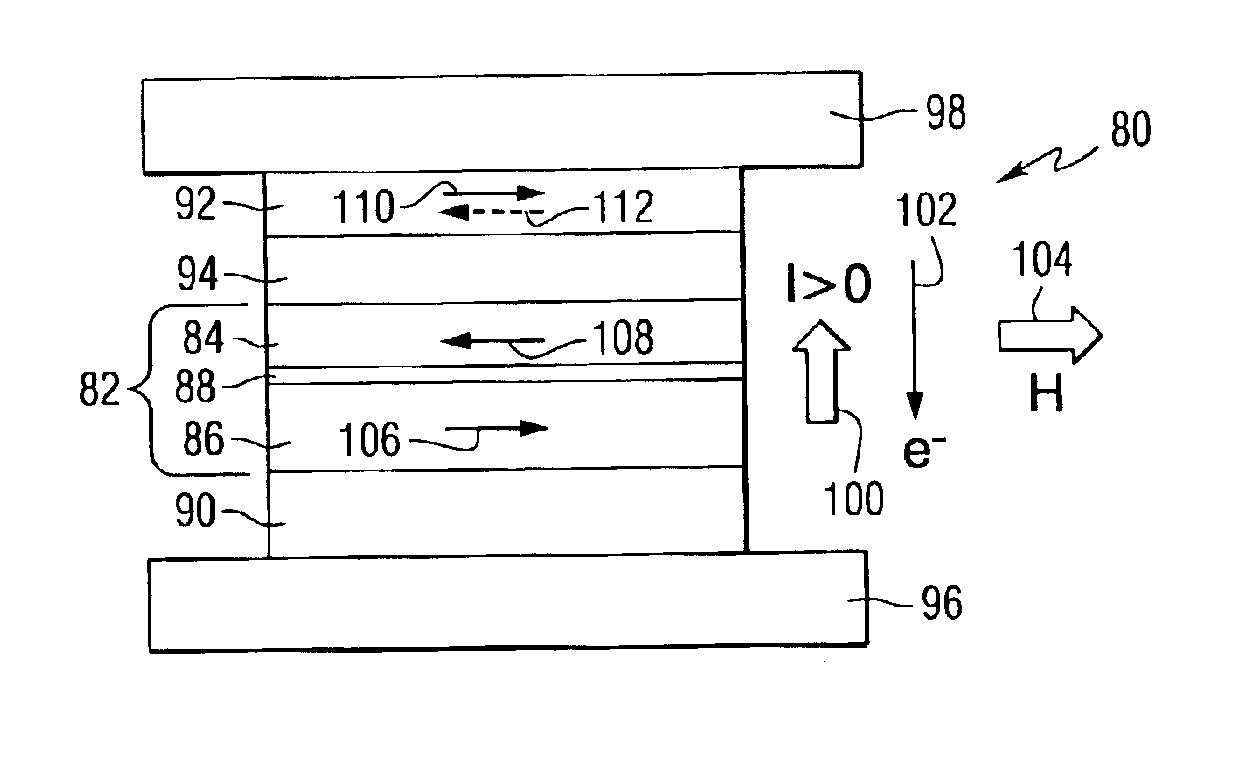
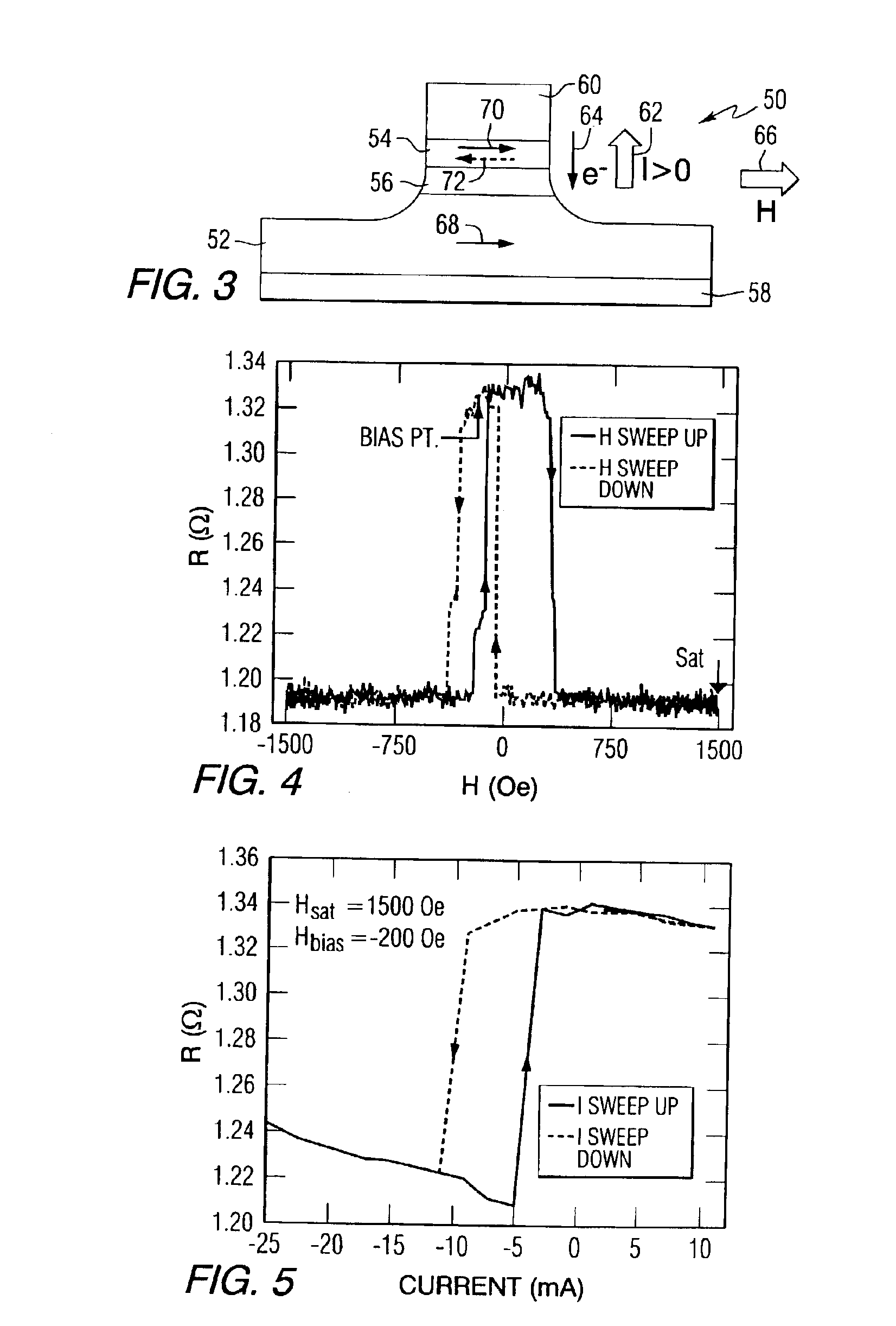
FIG. 2 is a cross-sectional view of a MR element 14, which for this particular example is a magnetic tunnel junction. The MR element is connected between a word line 16 and a bit line 22, and includes an antiferromagnetic layer 28, a pinned layer 30 positioned on the antiferromagnetic layer, a free layer 32, and a nonmagnetic layer 34 between the pinned layer and the free layer. The arrows 36 and 38 in the free layer, and arrow 40 in the pinned layer indic...


PUM


Abstract

A magnetic random access memory comprises a plurality of memory elements each comprising a magnetic pinned layer; a synthetic antiferromagnetic free layer including a first ferromagnetic layer, a second ferromagnetic layer, and a first nonmagnetic layer positioned between the first ferromagnetic layer and the second ferromagnetic layer, wherein the directions of magnetization of the first ferromagnetic layer and the second ferromagnetic layer are antiparallel; and a first conductive nonmagnetic layer positioned between the magnetic pinned layer and the synthetic antiferromagnetic free layer; and means for applying a current to each of the plurality of memory elements to affect the direction of magnetization of the synthetic antiferromagnetic free layer. A method of storing data using the magnetoresistive random access memory is also provided.

Description

FIELD OF THE INVENTIONThis invention relates to magnetic random access memories, and more particularly to magnetic random access memories that utilize a spin transfer write mechanism.BACKGROUND OF THE INVENTIONMagnetic random access memory, or MRAM, is a burgeoning new technology that will provide non-volatile data storage in a compact, low-power device. MRAM comprises an array of cells where each cell stores one bit in at least one magnetoresistive (MR) element. Bits are defined by the magnetic configuration of a free ferromagnetic layer (FL) within an MR element. The magnetic orientation of the FL with respect to a pinned ferromagnetic layer (PL) is measured via a magnetoresistive effect during read-back.MRAM technology is still in its infancy and has yet to reach the commercial market. Among the many challenges facing MRAM is the stabilization of a uniformly magnetized FL. Since common MRAM designs use magnetic fields generated by current carrying wires to write bits, the FL nece...

Claims


Application Information

Patent Timeline
Patent Type & Authority Patents(United States)
IPC IPC(8): G11C11/15G11C11/02
CPCG11C11/15
Inventor COVINGTON, MARK WILLIAM
Owner SEAGATE TECH LLC
Why Eureka
Try Eureka