

Color layer forming method
a color layer and forming method technology, applied in the field of color layer forming methods, can solve the problems of insufficient surface hardness of the color layer resist and the inability to produce color filters, and achieve the effect of reducing the time required and high producibility of the color filter
- Summary
- Abstract
- Description
- Claims
- Application Information
AI Technical Summary
Benefits of technology
Problems solved by technology
Method used
Image

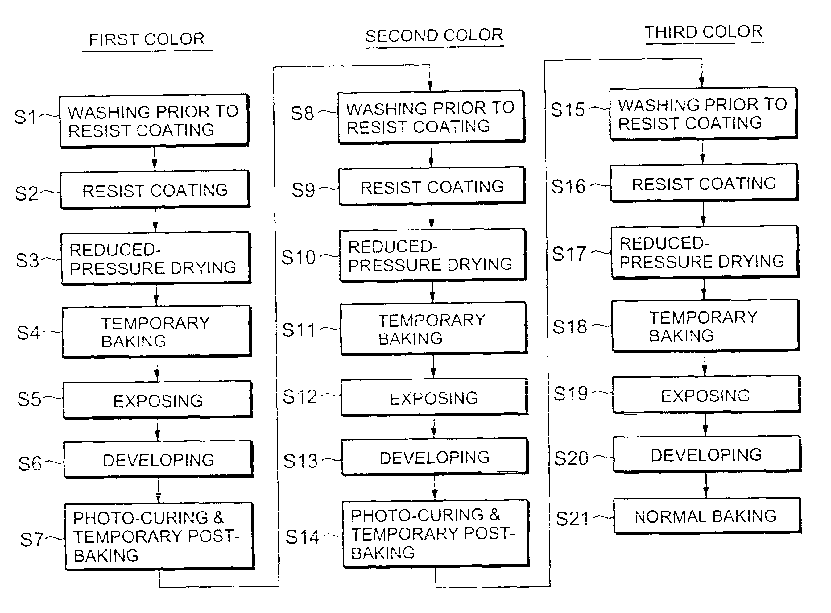
Examples
second embodiment
Now, the present invention will be described with reference to FIG. 5.
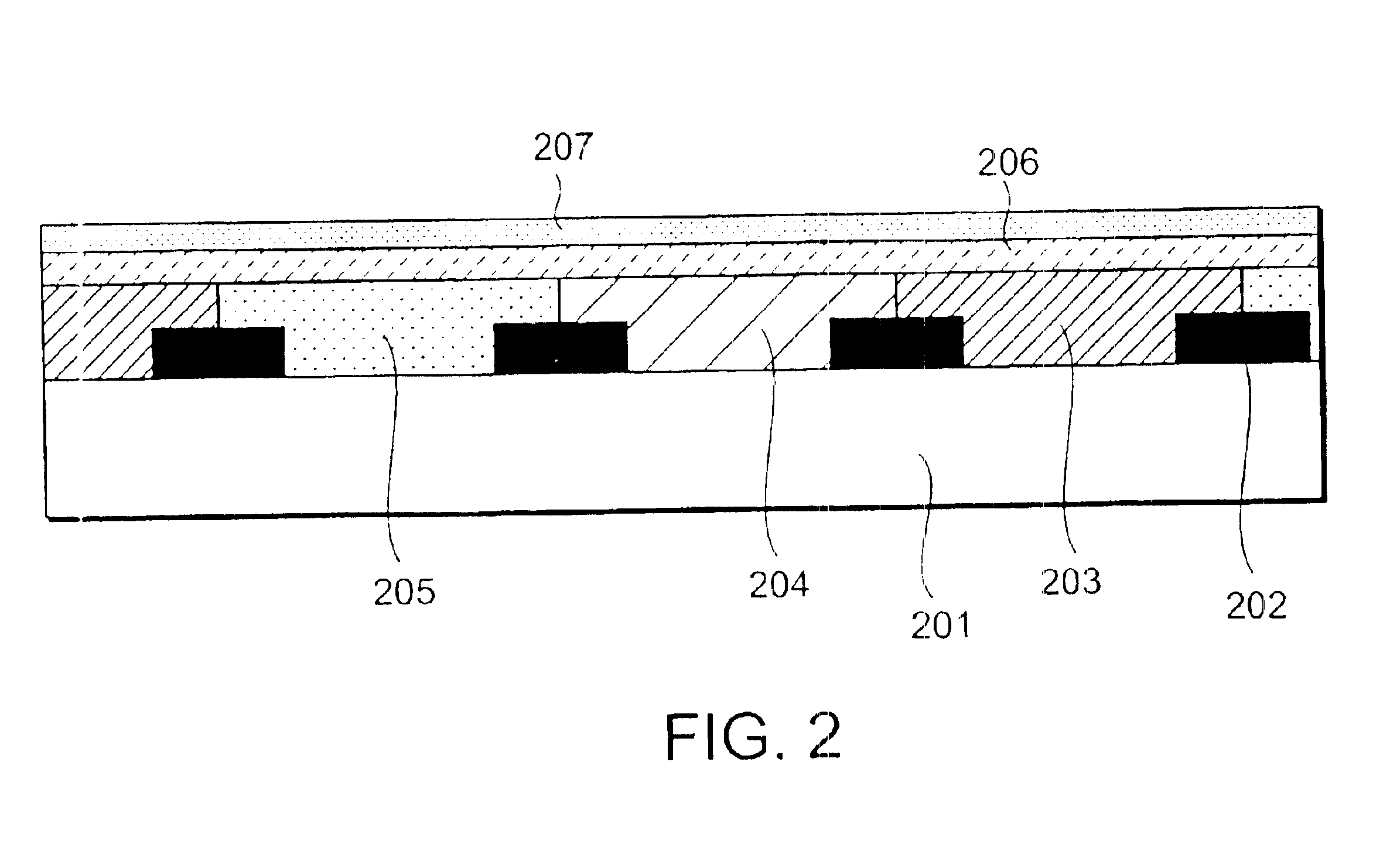
In the first embodiment, the color filter layer is formed on the usual transparent substrate. However, the present invention can be applied to a formation of a color filter layer on a thin film transistor (TFT).
In a TFT array substrate shown in FIG. 5, TFT's are formed by wiring portions 502 and amorphous silicon (a-Si) portions 503 formed on a transparent substrate 501. Metal film of such as chromium used as the wiring 502 is formed by sputtering, etc., and the a-Si portions 503 are formed by CVD, etc. On the TFT array substrate, a color layer composed of colored resists 504, 505 and 506 is formed along a fabrication procedure similar to that used in the first embodiment. A light shield layer 507 is formed of a metal or a black resist on the colored resists 504, 505 and 506 and, after a transparent organic interlayer film 508 is formed, pixel electrodes 509 of transparent conductive film are formed.
By forming the...
PUM
| Property | Measurement | Unit |
|---|---|---|
| temperature | aaaaa | aaaaa |
| temperature | aaaaa | aaaaa |
| color | aaaaa | aaaaa |
Abstract
Description
Claims
Application Information