Wafer defect inspection machine having a dual illumination system

a defect inspection machine and dual illumination technology, applied in the direction of optical elements, semiconductor/solid-state device testing/measurement, instruments, etc., can solve the problems of inability to illuminate the bottom part of the wafer pattern, inability to detect defects in the pits of the pattern, and image not so bright, etc., to achieve the effect of low cos

Inactive Publication Date: 2005-03-15
TOKYO SEIMITSU
View PDF2 Cites 21 Cited by
  • Summary
  • Abstract
  • Description
  • Claims
  • Application Information

AI Technical Summary

Benefits of technology

The objective of the present invention is to realize a defect inspection machine for semiconductor wafers that can detect various defects at a low cost.

Problems solved by technology

In the dark field illumination system, an image of extremely high contrast can be obtained, but there is a problem that the image is not so bright because the illumination light regularly reflected by the surface of the wafer 2 cannot be captured.
It is, therefore, impossible to illuminate the bottom part of the wafer pattern and a problem occurs that the defects in the pits of the patterns cannot be detected.
In the case of this inspection machine, as the bright field illumination system and the dark field illumination system are arranged between the objective lens 3 and the specimen 2, an objective lens of a large NA cannot be used and the projection magnification cannot be made large and, therefore, a problem occurs that this machine is not proper when inspecting defects in semiconductor wafer patterns.
As described above, a typical conventional defect inspection machine has a structure in which a dark field illumination system is provided outside the projection optical system, therefore, a problem occurs that it is not suitable as a defect inspection machine for semiconductor wafer that inspects fine patterns.
There occurs, however, a problem that the cost is increased if two illumination systems are provided and there is another problem particularly in the dark field illumination system that the cost is further increased because it is necessary to provide a ring-shaped condenser lens in addition to an objective lens.

Method used


Image

  • Wafer defect inspection machine having a dual illumination system
  • Wafer defect inspection machine having a dual illumination system
  • Wafer defect inspection machine having a dual illumination system

Examples


Embodiment Construction

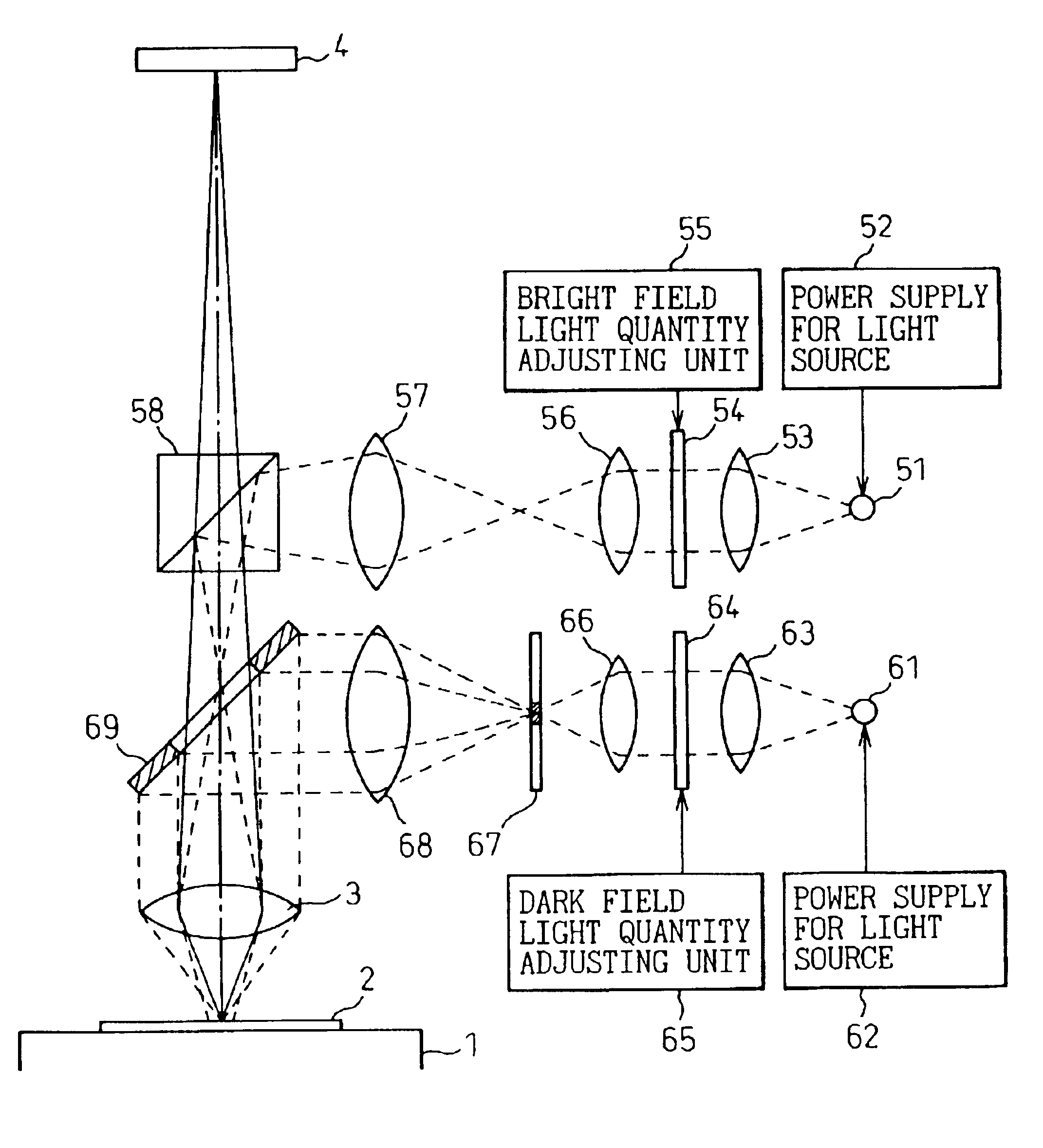
FIG. 4 is a diagram that shows the optical system of the defect inspection machine for semiconductor wafers in the embodiments of the present invention. Other parts shown in FIG. 1 are omitted here.

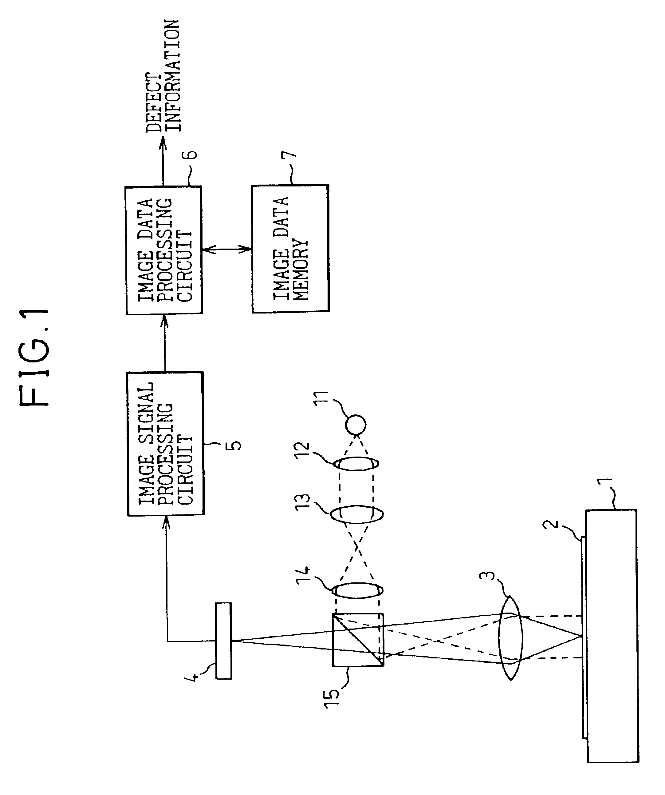
As shown in FIG. 4, the defect inspection machine for semiconductor wafers in the present embodiment comprises the stage 1 that holds the semiconductor wafer 2, the objective lens 3 that projects the optical image of the surface of the semiconductor wafer 2, the image sensor 4 that converts the projected optical image of the surface of the semiconductor wafer 2 into electric image signals, a bright field illumination system and a dark field illumination system. The bright field illumination system comprises a light source 51, a power supply for light source 52, an illumination lens 53, a light quantity adjusting filter 54, a bright field light quantity adjusting unit 55, illumination lenses 56 and 57 and a semi-transparent mirror (a beam splitter) 58. Although apertures can be provided as...


PUM

PropertyMeasurementUnit
defect inspectionaaaaaaaaaa
wafer defect inspectionaaaaaaaaaa
structureaaaaaaaaaa

Abstract

A low-cost defect inspection machine for semiconductor wafers that can detect various defects has been disclosed and comprises an optical system that projects a pattern image, an image sensor and a processing circuit that processes the image signal and detects defect portions, wherein the optical system comprises an objective lens, a bright field illumination system that has a semi-transparent mirror and irradiates a specimen through the objective lens with the illumination light reflected by the semi-transparent mirror in the range that includes the optical axis of the objective lens, and a dark field illumination system that has a reflecting mirror provided in the portion except for the projection path of the objective lens and irradiates a specimen through the objective lens with the illumination light reflected by the reflecting mirror.

Description

CROSS-REFERENCE TO RELATED APPLICATIONThis application claims priority of Japanese Patent Application No. 2001-351965, filed Nov. 16, 2001.BACKGROUND OF THE INVENTIONThe present invention relates to a wafer defect inspection machine that captures an image of a pattern formed on a wafer and detects a defective portion by processing image signals. More particularly, the present invention relates to a structure of an illumination optical system.Fixed patterns are formed repeatedly on semiconductor wafers, photomasks for semiconductor memories, liquid crystal display panels etc. In this case, optical images of these patterns are captured and defects of the patterns are detected by comparing neighboring patterns. If the result shows no difference between two patterns, it is judged that there is no defect in the two patterns, and if it shows a difference, it is judges that a defect exists in one pattern. As such a machine is generally called a wafer defect inspection machine, the term is ...

Claims


Application Information

Patent Timeline
Patent Type & Authority Patents(United States)
IPC IPC(8): G01N21/88G01N21/95G01N21/956G02B21/06G02B21/10G02B21/12H01L21/66
CPCG01N21/9501G01N2021/8825
Inventor KUROSAWA, TOSHIROUKATSUKI, YUZOTAKEBAYASHI, JUN
Owner TOKYO SEIMITSU
Why Eureka
Try Eureka