Semiconductor-on-insulator chip incorporating strained-channel partially-depleted, fully-depleted, and multiple-gate transistors

a technology of semiconductors and insulators, applied in the direction of semiconductor devices, electrical equipment, transistors, etc., can solve the problems of reducing affecting the design of the circuit using pd-soi devices, and affecting the electrical performance of the circuit, so as to reduce the effect of floating body effects and magnify the effect of high-stress film on channel strain

Inactive Publication Date: 2005-03-15
TAIWAN SEMICON MFG CO LTD
View PDF44 Cites 324 Cited by
  • Summary
  • Abstract
  • Description
  • Claims
  • Application Information

AI Technical Summary

Benefits of technology

In one embodiment, the present invention provides a method and system that overcomes the shortcomings of the prior art, and provides a highly manufacturable PD-SOI-like technology that produces FD-SOI type devices to eliminate floating body effects. Other embodiments of the invention provide a novel transistor geometry to magnify the effect of high-stress film on the channel strain. The present disclosure teaches a method of forming such a transistor.

Problems solved by technology

Although PD-SOI devices have the merit of being highly manufacturable, significant design burdens are faced by its users because of floating body effects.
This results in kinks in the device current-voltage (I-V) curves, thereby degrading the electrical performance of the circuit.
Therefore, circuit design using PD-SOI devices is not straightforward, and there is a significant barrier for the adoption of PD-SOI technology or the migration from bulk-Si design to PD-SOI design.
Various methods of making a contact to the body of a SOI transistor are known, but various disadvantages are known to be associated with these methods.
However, the method is limited by a high body contact resistance.
However, raised source / drain formation, currently performed by selective epitaxy, is immature, expensive, pattern-density dependent, and may result in reduced manufacturing yield.
In addition, SOI substrates with uniform ultra-thin Si films, as required for the manufacture of FD-SOI devices with ultra-thin body, are currently unavailable.
Non-uniformity of the Si film thickness will result in significant fluctuations in the device characteristics and negatively impact the ease of manufacture.

Method used


Image

  • Semiconductor-on-insulator chip incorporating strained-channel partially-depleted, fully-depleted, and multiple-gate transistors
  • Semiconductor-on-insulator chip incorporating strained-channel partially-depleted, fully-depleted, and multiple-gate transistors
  • Semiconductor-on-insulator chip incorporating strained-channel partially-depleted, fully-depleted, and multiple-gate transistors

Examples


Embodiment Construction

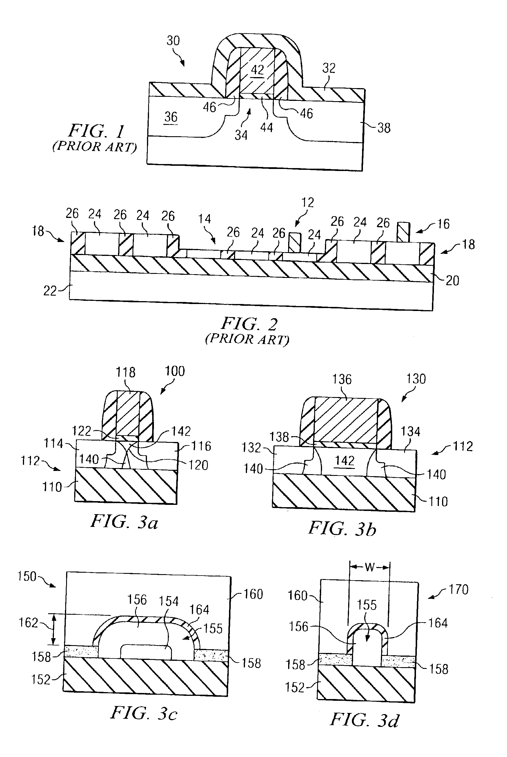
The present invention is related to co-pending applications Ser. No. 10 / 305,841 entitled “Strained-Channel Multiple-Gate Transistor”, filed Nov. 26, 2002 and Ser. No. 10 / 319,119 entitled “Semiconductor-on-Insulator Chip Incorporating Partially-Depleted, Fully-Depleted, and Multiple-Gale Devices”, filed Dec. 12, 2002. Aspects of the present invention provide improvements.

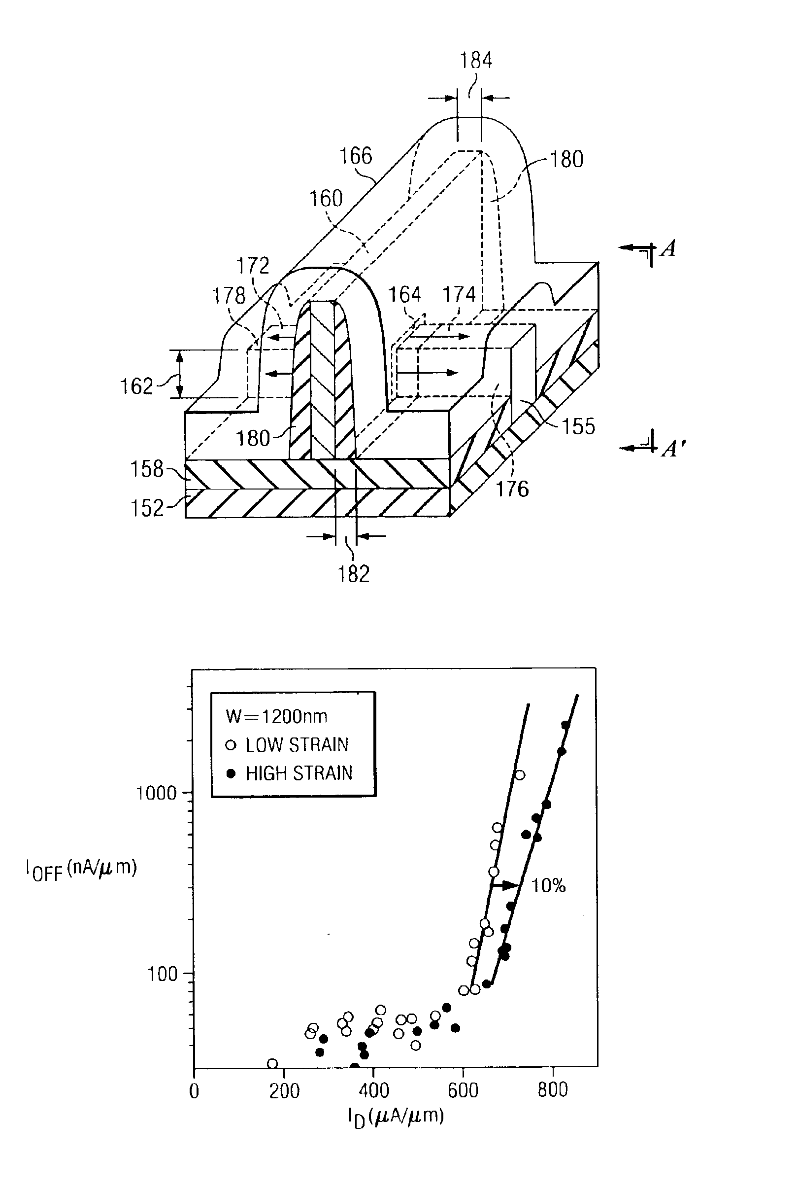
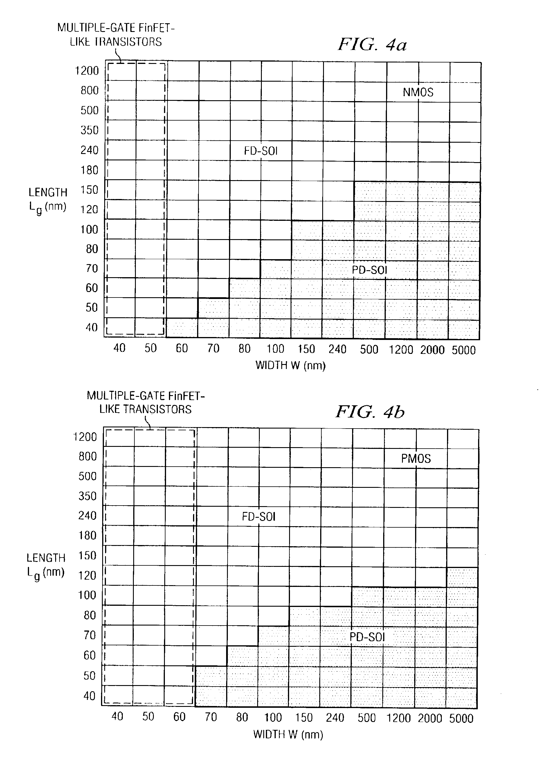
For example, the preferred embodiment of the present invention teaches a method and architecture to incorporate partially-depleted SOI (PD-SOI) and fully-depleted SOI (FD-SOI) transistors in the same chip, and, to provide enhanced strain effects to improve carrier mobilities and device performance in ultra-scaled devices. Unlike other devices that utilize different silicon thicknesses to the achieve FD-SOI and PD-SOI transistors on the same chip, the preferred embodiment of the present invention employs a PD-SOI technology while implementing FD-SOI transistors by rearranging the transistor geometry, or by configuring...


PUM


Abstract

In accordance with a preferred embodiment of the present invention, a silicon-on-insulator (SOI) chip includes a silicon layer of a predetermined thickness overlying an insulator layer. A multiple-gate fully-depleted SOI MOSFET including a strained channel region is formed on a first portion of the silicon layer. A planar SOI MOSFET including a strained channel region formed on another portion of the silicon layer. For example, the planar SOI MOSFET can be a planar fully-depleted SOI (FD-SOI) MOSFET or the planar SOI MOSFET can be a planar partially-depleted SOI (PD-SOI) MOSFET.

Description

TECHNICAL FIELDThe present invention relates generally to the fabrication of semiconductor devices. More particularly, the preferred embodiment of the present invention relates to semiconductor-on-insulator chips incorporating partially-depleted, fully-depleted, and multiple-gate devices, and the introduction of strain in the channel of these devices.BACKGROUNDSemiconductor device geometries have dramatically decreased in size since such devices were first introduced several decades ago. Since then, integrated circuits have generally followed the two year / half-size rule (often called Moore's Law), which means that the number of devices on a chip doubles every two years. Today's semiconductor fabrication plants are routinely producing devices having 130 nm and even 90 nm feature sizes.The desire for higher performance circuits has driven the development of high-speed sub-100 nanometer (nm) silicon-on-insulator (SOI) complementary metal-oxide-semiconductor (CMOS) technology. In SOI te...

Claims


Application Information

Patent Timeline
Patent Type & Authority Patents(United States)
IPC IPC(8): H01L21/70H01L27/12H01L21/84H01L21/336H01L29/786
CPCH01L21/84H01L27/1203H01L29/66795H01L29/7854H01L29/7843H01L29/785H01L29/7842
Inventor YEO, YEE-CHIACHEN, HOW-YUHUANG, CHIEN-CHAOLEE, WEN-CHINYANG, FU-LIANGHU, CHENMING
Owner TAIWAN SEMICON MFG CO LTD
Why Eureka
Try Eureka